July 24, 2013
By Sarah Yang
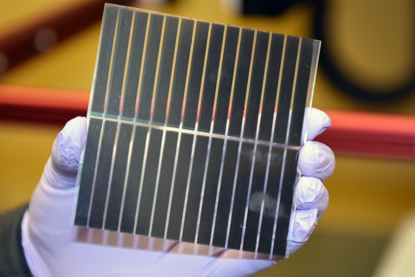
BERKELEY — Engineers at the University of California, Berkeley, have developed an inexpensive new way to grow thin films of a material prized in the semiconductor and photovoltaic industries, an achievement that could bring high-end solar cells within reach of consumer pocketbooks.
The work, led by Ali Javey, UC Berkeley associate professor of electrical engineering and computer sciences, is described in a paper published today (Wednesday, July 24) in Scientific Reports, Nature’s peer-reviewed open access journal.
“Performance is everything in the solar cell industry, but performance at a reasonable cost is key,” said Javey, who is also a faculty scientist at the Lawrence Berkeley National Laboratory. “The techniques we are reporting here should be a game-changer for III-V solar cells, as well as for LEDs.”
Top of the line photovoltaics are made from a class of material known as III-V (pronounced “three-five”) compounds, known for their superior efficiency at converting light into power. However, the complex manufacturing requirements for III-V materials make them up to 10 times more expensive than silicon, limiting their use to military applications and NASA satellites, the researchers said.
The UC Berkeley researchers demonstrated that indium phosphide, a III-V compound, could be grown on thin sheets of metal foil in a process that is faster and cheaper than traditional methods, yet still comparable in opto-electronic characteristics.
The paper’s co-lead authors from Javey’s lab are Rehan Kapadia, a recent Ph.D. graduate, and Zhibin Yu, a post-doctoral researcher.
The U.S. Department of Energy helped fund this research.
MORE INFORMATION
A direct thin-film path towards low-cost large-area III-V photovoltaics (Link to Scientific Reports paper)


