February 26, 2014>
Researchers from North Carolina State University have developed a “superabsorbing” design that may significantly improve the light absorption efficiency of thin film solar cells and drive down manufacturing costs.
The superabsorbing design could decrease the thickness of the semiconductor materials used in thin film solar cells by more than one order of magnitude without compromising the capability of solar light absorption.
“State-of-the-art thin film solar cells require an amorphous silicon layer that is about 100 nanometers (nm) thick to capture the majority of the available solar energy,” says Dr. Linyou Cao, an assistant professor of materials science and engineering at NC State and senior author of a paper describing the work. “The structure we’re proposing can absorb 90 percent of available solar energy using only a 10 nm thick layer of amorphous silicon.
“The same is true for other materials. For example, you need a cadmium telluride layer that is one micrometer thick to absorb solar energy, but our design can achieve the same results with a 50 nm thick layer of cadmium telluride. Our design can also enable a 30 nm thick layer of copper indium gallium selenide to fully absorb solar light. That’s a huge advance.”
Cao notes that the deposition of semiconductor materials stands as a major bottleneck for improving manufacturing productivity and lowering the cost of thin film solar cells. “A decrease in the thickness of semiconductor materials by one order of magnitude would mean a substantial improvement in manufacturing productivity and reduction in cost,” Cao says, because the cells would use less material and the thin films could be deposited more quickly.
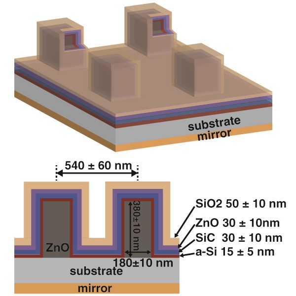
In cross-section, the new design looks like a rectangular onion. The light-absorbing semiconductor material coats a rectangular core. The semiconductor, in turn, is coated by three layers of anti-reflective coating that do not absorb light.
To develop the design, the researchers began by examining the maximum light absorption efficiency of semiconductor materials using light-trapping techniques. They found that maximizing solar absorption requires a design in which the light-trapping efficiency for solar light is equal to the intrinsic absorption efficiency of the semiconductor materials. In other words, in order to maximize solar absorption, you need to match the amount of solar light trapped inside the structure and the amount of solar light that could be absorbed. The researchers then designed the onion-like structures to match their light-trapping efficiency with the absorption efficiency of the semiconductor materials in thin film solar cells.
“We first theoretically predicted the maximum solar light absorption efficiency in given semiconductor materials, and then proposed a design that could be readily fabricated to achieve the predicted maximum. We developed a new model to do this work, because we felt that existing models were not able to find the upper limit for the solar absorption of real semiconductor materials,” Cao says “And if this works the way we think it will, it would fundamentally solve light-absorption efficiency problems for thin film solar cells.
“The superabsorbing structure is designed for the convenience of fabrication, and we are looking for partners to produce and test this design,” Cao adds. “The structure should be very easy to produce with standard thin film deposition and nanolithography techniques. We are happy to work with industry partners to implement this design in the production of next-generation solar cells.”
The paper, “Semiconductor Solar Superabsorbers,” was published Feb. 17 in the journal Scientific Reports. Lead author of the paper is Yiling Yu, a Ph.D. student at NC State. The paper was co-authored by NC State Ph.D. student Lujun Huang.
Abstract:
“Semiconductor Solar Superabsorbers”
Authors: Yiling Yu, Lujun Huang, and Linyou Cao, North Carolina State University
Published: Feb. 17, 2014, Scientific Reports
DOI: 10.1038/srep04107
Abstract: Understanding the maximal enhancement of solar absorption in semiconductor materials by light trapping promises the development of affordable solar cells. However, the conventional Lambertian limit is only valid for idealized material systems with weak absorption, and cannot hold for the typical semiconductor materials used in solar cells due to the substantial absorption of these materials. Herein we theoretically demonstrate the maximal solar absorption enhancement for semiconductor materials and elucidate the general design principle for light trapping structures to approach the theoretical maximum. By following the principles, we design a practical light trapping structure that can enable an ultrathin layer of semiconductor materials, for instance, 10 nm thick a-Si, absorb > 90% sunlight above the bandgap. The design has active materials with one order of magnitude less volume than any of the existing solar light trapping designs in literature. This work points towards the development of ultimate solar light trapping techniques.

