March 24, 2017
WASHINGTON — A new fabrication process could make it easier and less expensive to incorporate optical sensing onto lab-on-a-chip devices. These devices integrate laboratory functions onto a plastic or glass “chip” typically no more than a few square centimeters in size, allowing automated testing in the doctor’s office or various types of chemical or biological analysis with portable instruments.
The most common material used to make lab-on-a-chip devices today is the silicone poly-dimethylsiloxane (PDMS) because of its optical, mechanical and chemical properties, its low cost and the ease at which it can be structured at the microscale. As these devices become more common and increasingly complex, there is a need for less expensive ways to incorporate all-PDMS optical components such as waveguides to direct light onto and within the chip.
“Our new method is compatible with the development of lab-on-chip platforms where integrated optical waveguides can be a great tool for light-based diagnostics or monitoring applications,” said Mathieu Hautefeuille of Universidad National Autonomous University of Mexico, co-author of the paper.
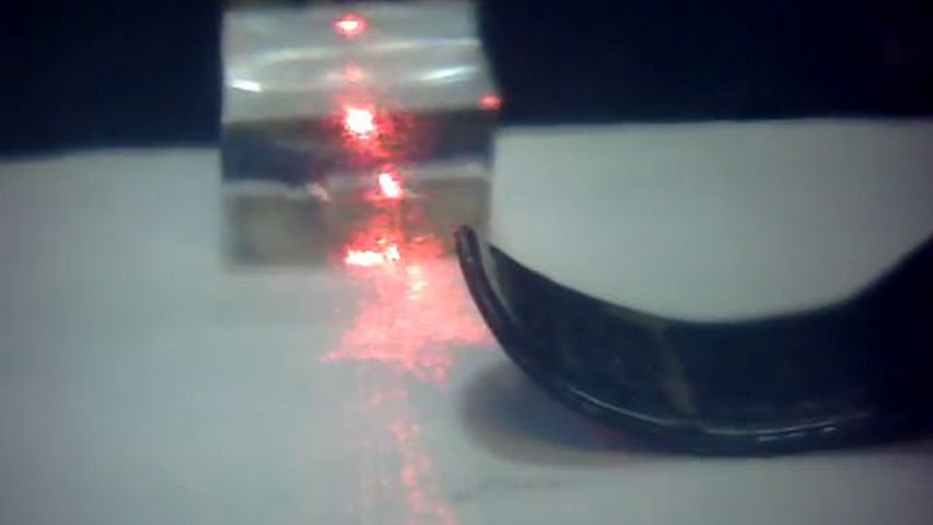
In the journal Optical Materials Express, from The Optical Society (OSA), the researchers describe their simple and inexpensive method for making PDMS waveguides that can be easily integrated into a lab-on-a-chip device made of the same material. They use their new approach to fabricate a PDMS beam splitter, which splits laser output into two beams.
“To the best of our knowledge, this is the first time that low-power laser etching has been used to microstructure polymers for optical waveguide fabrication,” said Hautefeuille. “This study shows that a very inexpensive laser platform, based on a CD/DVD unit in our case, can compete with high-power lasers for such applications.”
The researchers say that their new fabrication technique could be useful for other applications, including those requiring precision microstructuring, and that it can be used to etch other polymer materials in addition to PDMS.
Low-power etching of a transparent material
To make the PDMS waveguides, the researchers began by creating a mold. They used the strongly focused laser beam of a CD/DVD burner they had on hand to etch a clear sheet of acrylic. Because low-power laser sources like the ones in CD/DVD burners typically aren’t absorbed by transparent materials, the researchers coated the acrylic with highly absorbent nanocarbon. This created pinpoint areas of intense heat that could be used to etch the material with micro-scale resolution.
The researchers next created PDMS with two different indices of refraction by carefully modifying the mixing and curing conditions of the material. They filled the etched micromold with PDMS of one refractive index, cured the material, then placed a layer of PDMS with a different refractive index on top. After another curing step, the researchers removed the PDMS from the mold, flipped it and added another layer of PDMS to create a waveguide completely embedded into two slabs of PDMS.
To verify the reproducibility of the mixing and curing recipe used to control the optical properties of PDMS, the researchers measured the refractive index of their fabricated PDMS layers several times. They also showed that the optical losses of waveguides made with this technique matched those reported for more complicated fabrication techniques.
“In addition to being low-cost, our technique accomplishes rapid prototyping of waveguides that can make it possible to integrate light-based capabilities such as interferometric devices into lab-on-a-chip devices,” said Hautefeuille. “It is also possible to fabricate long waveguides with our method, which can be a great advantage in lab-on-chip devices.”
Making a PDMS beam splitter
Using the new approach, the researchers fabricated an 8-millimeter long, Y-shaped beam splitter. In addition to demonstrating that the beam splitter separated a laser beam into the two output arms, the researchers also showed that the light could be switched between each arm by changing the position and angle of the optical fiber delivering the light.
The researchers are now working to demonstrate that their method can be used to fabricate more complex integrated optical devices such as an interferometer that could serve as an all-PDMS platform for sensing applications.
The team’s success with this approach breathes new life into older technology while showing that high precision doesn’t always require expensive, cutting-edge equipment. “Our study shows that short-pulsed lasers are not strictly necessary to etch transparent polymers and plastics with a micron-scale resolution,” said Hautefeuille. “The use of a recycled CD/DVD unit further shows that you might be able to stretch the usage of equipment that could be starting to look out of date.”
This project was supported by DGAPA-PAPIIT and CONACyT grants as well as the Red Temática de Biofotónica, CONACyT.
Paper: D. Pérez-Calixto, D. Zamarrón-Hernández, A. Cruz-Ramírez, M. Hautefeuille, J. Hernández-Cordero, V. Velázquez, M. Grether, “Fabrication of large all-PDMS micropatterned waveguides for lab on chip integration using a rapid prototyping technique,” Opt. Mater. Express Volume 7, Issue 4, 1343-1350 (2017).
DOI: 10.1364/OME.7.001343

