March 9, 2021
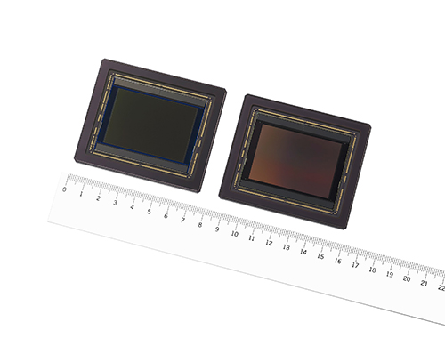
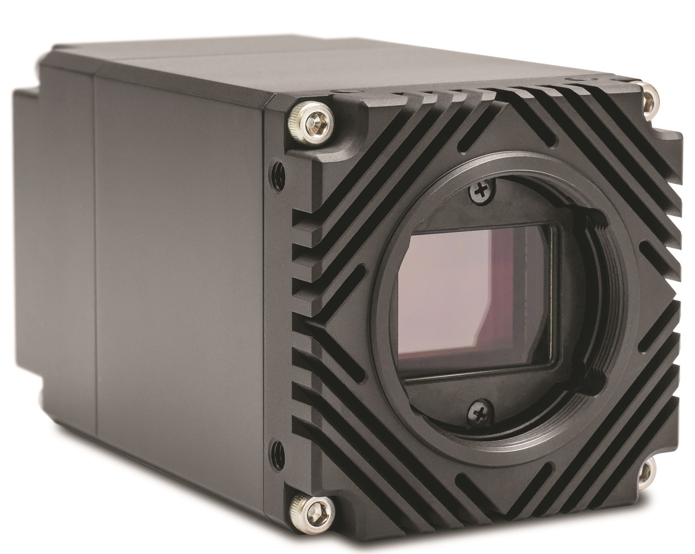
Tokyo, Japan — Sony Corporation announced today the upcoming release of a large format 56.73mm diagonal CMOS image sensor "IMX661" for industrial equipment with a global shutter function and the industry's highest effective pixel count of 127.68 megapixels.
This product features an increased pixel count that yields an optical size nearly 10 times larger than the common 1.1-type image sensor corresponded to the C mount for industrial equipment. It also features Sony's original global shutter pixel technology "Pregius™", which enables capture of motion distortion-free images. Furthermore, the Sony's original device configuration and interface technology employed enable high-speed image readout at a data rate nearly four times faster than conventional products.
Sony expects that the new sensor, when used in industrial equipment cameras for a wide variety of applications, will help to solve a variety of complex challenges, thereby contributing to the development of industry.
Needs for automation, labor-saving and other benefits of digital transformation continue to grow in recent years in various fields of industrial equipment. This has accelerated the adoption of cameras for a wide variety of applications, driving demand for CMOS image sensors with higher imaging performance.
The new product couples Sony's Pregius technology with the 3.6-type (56.73mm diagonal) large optical size, delivering an increased pixel count and motion distortion-free imaging. The original device configuration, which employs a chip-on-wafer process, together with Sony's original interface technology, enables high-speed readout nearly four times faster than conventional products in full-pixel readout mode. This design delivers highly efficient imaging that captures a wide viewing angle with no motion distortion in a single imaging operation. It also improves recognition precision thanks to the high-resolution imaging and delivers a high level of processing performance. It can contribute to solutions for a variety of industrial equipment applications, for example, inspection processes for production of displays and electronic substrates, wide-area monitoring, and aerial photography, where its improved precision and quicker readout will help meet the need for a high level of productivity.
The industry’s highest effective pixel count of 127.68 megapixels
This product features a large optical size of 3.6-type (56.73mm diagonal), nearly 10 times larger than the common 1.1-type image sensor corresponded to the C mount lens for industrial equipment with a pixel size of 3.45 μm, resulting in a massive pixel count of 127.68 megapixels, which is the industry's highest for a CMOS image sensor equipped with a global shutter. It enables a wide viewing angle and high-resolution imaging by increased pixel count, and the motion distortion-free imaging demanded on cameras for industrial equipment, thereby improving imaging efficiency and recognition precision.
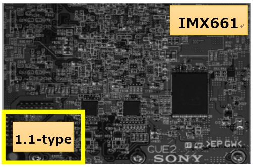
Image sensor optical size (imaging area) comparison, area ratio about 10 times (1.1-type comparison)
High-speed image readout
Generally, increased pixel count means increased signal processing volume, which causes issues such as a drop in frame rate and longer readout times. In order to realize high-speed readout, it is necessary to improve the processing functionality of the AD converter which converts the analog signal output from the pixel to digital signals, and at the same time, increase the speed of the output interface.
This product features Sony's original device configuration employing a chip-on-wafer process where chips with certain functions are stacked on top of the pixel wafer, allowing for optimal positioning of the AD converter. This design improves AD converter processing functionality without increasing the size.
The new sensor also employs the Scalable Low Voltage Signaling with Embedded Clock (SLVS-EC™) high-speed interface standard developed by Sony, in order to make output interface faster. These two original technologies enable 127.68 megapixels,10bits,21.8fps, which is a high-speed output data rate nearly four times faster than conventional models.The dramatic increase in multi-pixel and readout speed greatly contribute to the improvement of productivity in industrial applications.
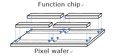
Device configuration using chip-on-wafer process
Equipped with signal processing capabilities needed for a variety of industrial applications
The new product is equipped with a range of signal processing capabilities required for industrial equipment CMOS image sensors to meet diverse applications and needs. These include such as; trigger synchronization for controlling imaging timing during high-speed inspections; Region of Interest (ROI), which reduces post signal processing load by only reading out the required regions; gradation compression, which reduces data volume while outputting required information; multi-exposure, which is capable of detecting the trajectory of moving objects; short exposure time for blur-free imaging of objects moving at high speeds; pixel binning readout, which can enhance sensitivity in low luminance situations.

