LEUVEN (Belgium), OCT 21, 2019 — Imec, a world-leading research and innovation hub in nanoelectronics and digital technology, presents a new thin-film monolithic image sensor that captures light in the near-infrared (NIR) and short-wavelength infrared (SWIR). Based on a monolithic approach, the process promises an order of magnitude gain in fabrication throughput and cost compared to processing today’s conventional IR imagers, while at the same time enabling multi-megapixel resolution. IR imagers are used in a wide variety of applications, and imec’s new technology greatly extends their possibilities, including surveillance, biometric identification, virtual reality, machine vision, and industrial automation.

Monolithic thin-film image sensor for the SWIR range, processed at die level. Imec works towards scaling the process to wafer level which increases throughput and cost compared to today’s conventional IR imagers, while at the same time enabling multi-megapixel resolution.
To date, infrared image sensors are produced through a hybrid technology: the crystalline semiconductor detector and the electronic readout are fabricated separately and then interconnected at pixel or chip periphery level. This is an expensive and time-consuming process with a low throughput, resulting in sensors with a restricted resolution that often require cooling to reduce the signal noise under dark conditions. This prevents a widespread use of IR imagers in consumer applications. For some time, researchers have been looking at various monolithic approaches. Imec’s approach paves the way to high-resolution, low-cost, wafer-based SWIR imagers.
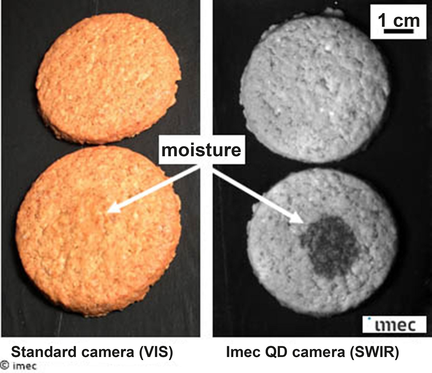
Test images of cookies acquired with a standard Si-based camera in visible range (left) and imec QD-based camera at the wavelength of 1450 nm (right). Bottom cookie had a drop of water applied to its surface, which can be only distinguished in the SWIR thanks to high water absorption contrast.
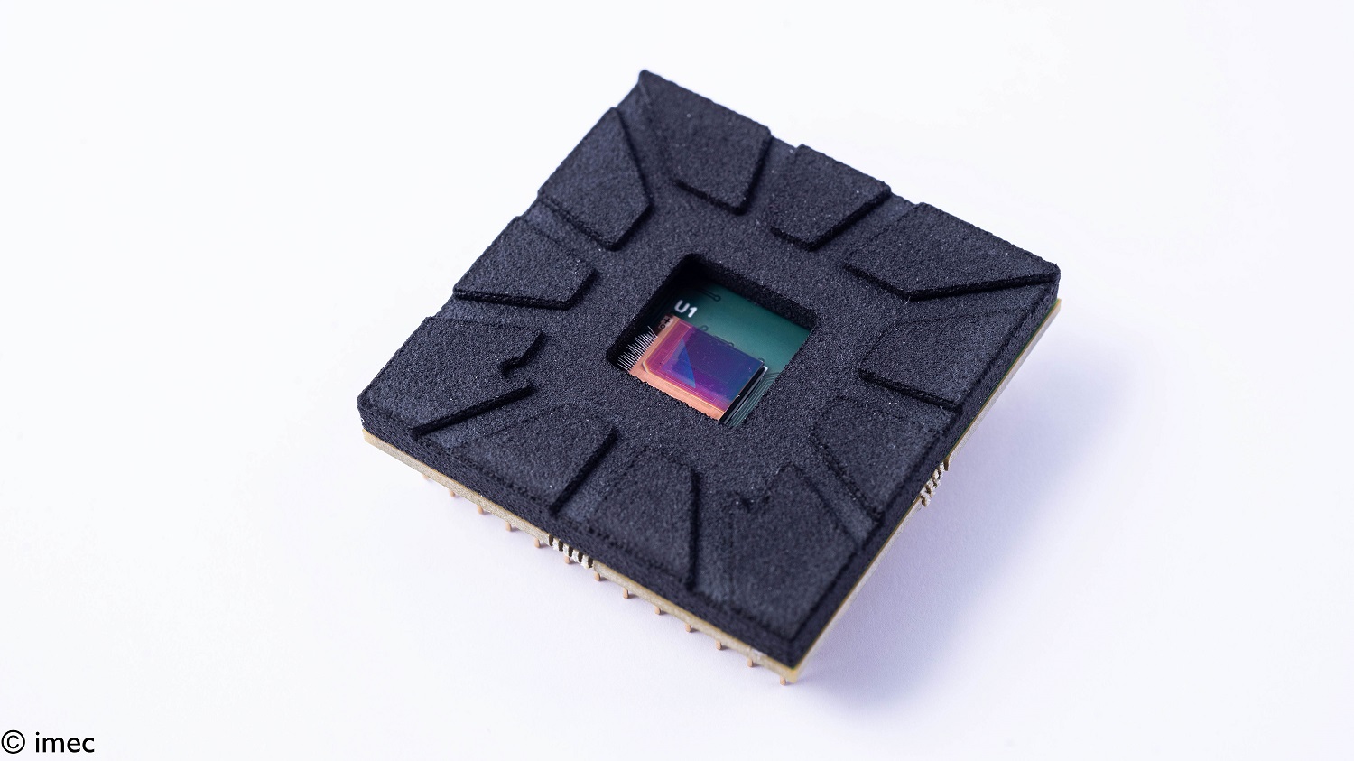
Imec's IR imagers consist of a novel thin-film photodetector pixel stack based on quantum dots deposited directly on top of an electronic readout. They are manufactured in a monolithic process compatible with wafer-based mass production. The pixels embed newly developed high-performance low bandgap quantum dot materials that match or even surpass the performance of inorganic light absorbers. The stacks have been carefully engineered and can be tuned to target a spectrum from visible light all the way up to 2µm wavelength. Test photodiodes on silicon substrate achieve an external quantum efficiency above 60 percent at 940nm wavelength, exceeding the state-of-the-art, and above 20 percent at 1450nm, allowing for uncooled operation with dark current comparable to commercial InGaAs photodetectors. The prototype imager has resolution of 758x512 pixels and 5um pixel pitch.
“We are excited to present this outstanding thin-film imager, a collaborative result of several teams with expertise ranging from chemistry, device engineering, readout design through integration and fab manufacturing. This result opens up many new applications for thin-film imagers,” commented Pawel Malinowski, imec’s thin-film imagers program manager. “Our imagers could be integrated in next generation world-facing smartphone cameras coupled with eye-safe light sources, enabling compact sensing modules for augmented reality. In inspection, they could be used for food or plastics sorting, and in surveillance for low-light cameras with better contrast. Additionally, by enabling feature distinction in bad weather or smoke conditions, one can envision firefighting applications and, in the future, Advanced Driver Assistance Systems (ADAS).”
Wafer with image sensors for the SWIR range. Processed at wafer-scale, these thin-film imagers can be produced with increased throughput and cost compared to today’s conventional IR imagers, while at the same time enabling multi-megapixel resolution.
Looking further, imec aims to develop a wafer-level NIR and SWIR image sensor technology and develop technologies for companies with a roadmap in innovative image sensors, cameras and smart imaging applications. The current SWIR photodetector is the result of several collaborations, including the Flemish VLAIO-SBO project MIRIS (IWT/150029) with academic partners Ghent University and University of Hasselt, and Flanders based companies active in imaging technology.