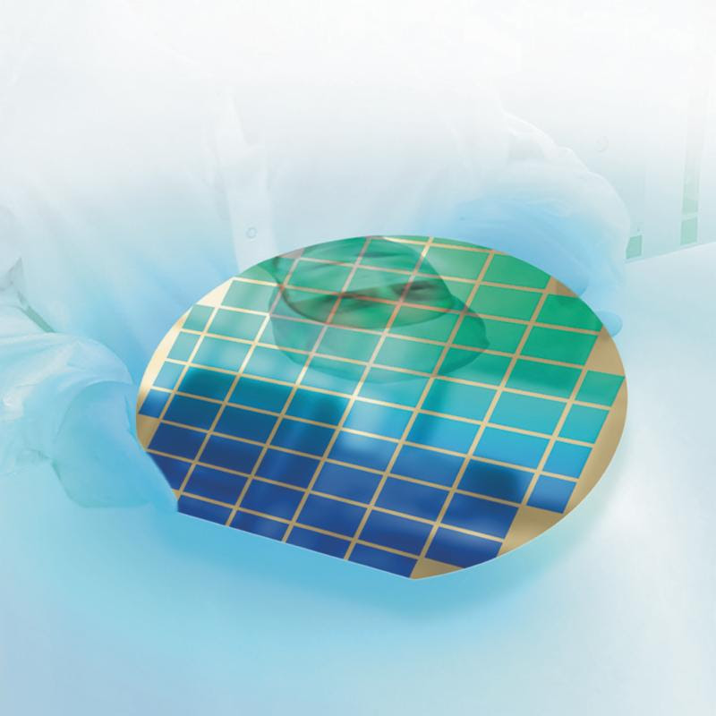
San Jose, Calif., USA - 8 March, 2018. Testing CMOS image sensors on a wafer-size scale is not easy because of the challenges of creating uniform illumination over a large area. Presto Engineering has developed a custom, computer-controlled solution that illuminates sections of the wafer in turn. Integrating the results enables the whole wafer to be tested automatically for an array of large sensors or even sensors that are right up to the size of an entire 12-inch wafer.
"An entire wafer can be tested in a laboratory using a similar method," explained Martin Kingdon, Presto Engineering's VP of Sales. "However laboratories are not geared up for fast commercial testing so we designed our own solution to test any size wafer. Importantly, we can do this in small to medium sized test runs here in Europe at our Class 10K cleanroom facility in Meyreuil, France, near Aix-en-Provence. We believe that we are probably the only such commercial test service to be available in Europe."
Commercial testing of small image sensors is very easy as the small areas involved are easy to illuminate with a controlled, uniform test pattern of light. But, as the area increases, it becomes harder to maintain the uniformity across the test area of an individual sensor due to the limitation of the optics. By illuminating sections of the wafer in turn, Presto is able to merge the results together to test the functionality of the image sensors on the wafer.
The need for larger image sensors is being driven, in particular, by medical imaging and aerospace that can require whole wafer-sized, image sensors and are transitioning from CCD to CMOS solutions. Similarly, security and military applications, etc. are all wanting larger, better sensors to provide the resolution required to provide clear sharp images, as well as other 4K resolution cameras. The tester is located in Presto's EAL 5/6+ facilities so that it meets the security needs of sensitive applications.
Presto's Teradyne® IP750Ex based test solution provides a large (80x100mm), uniform (+/-2%), high-intensity illumination field up to 10K Lux at a range of colour temperatures. Built-in IR filtering prevents sensor damage. Its ability create a customised test solution for complex devices (as large as 32M pixels at speeds up to 200MHz) on up to 12-inch wafers enables fast ramps without compromising cost-of-test.
Presto Engineering will be attending the conference at Image Sensors Europe 2018 on the 14th and 15th March 2018. www.image-sensors.com
More information about Presto Engineering can be found at www.presto-eng.com

