December 8, 2015
By Carla Reiter
More than a decade ago, theorists predicted the possibility of a nanolens—a chain of three nanoscale spheres that would focus incoming light into a spot much smaller than possible with conventional microscopy. Such a device would make possible extremely high-resolution imaging or biological sensing. But scientists had been unable to build and arrange many nanolenses over a large area.
“That’s where we came in,” said Xiaoying Liu, senior research scientist at the University of Chicago’s Institute for Molecular Engineering. Liu and Paul Nealey, the Dougan Professor in Molecular Engineering, teamed with experts in nanophotonics at the Air Force Research Laboratory and Florida State University to invent a novel way to build nanolenses in large arrays using a combination of chemical and lithographic techniques.
They aligned three spherical gold nanoparticles of graduated sizes in the string-of-pearls arrangement predicted to produce the focusing effect. The key, said Liu, was control: “We placed each individual nanoparticle building block into exactly the position we wanted it to go. That’s the essence of our fabrication technique.”
The team described its technique in the latest edition of Advanced Materials. The first step employs the lithographic methods used in making printed circuits to create a chemical mask. Liu and Nealey’s mask leaves exposed a pattern of three spots of decreasing size on a substrate such as silicon or glass that won’t absorb the gold nanoparticles.
Delicate patterns
Lithography allows for extremely precise and delicate patterns, but it can’t produce three-dimensional structures. So the scientists used chemistry to build atop the patterned substrate in three dimensions. They treated the spots with polymer chains that were then tethered to the substrate through chemical bonds.
“The chemical contrast between the three spots and the background makes the gold particles go only to the spots,” said Liu. To get each of the three sizes of nanospheres to adhere only to its own designated spot, the scientists played with the strength of the chemical interaction between spot and sphere. “We control the size of the different areas in the chemical pattern and we control the interaction potential of the chemistry of those areas with the nanoparticles,” said Nealey.
Only the largest spot has the amount of force needed to attract and hold the largest particle; the interaction of the particle with the middle and the small spots is too weak.
When the big spheres are adsorbed, the scientists use the same trick to put the medium-sized spheres onto the medium-sized spots, and finally move on to the smallest.
“It’s like the Three Bears story,” said Nealey. “We can put big ones on the big spots, but they won’t stick to the smaller spots; then put the next-sized one on the medium spot, but it won’t stick to the small spot. By this sequential manufacturing we’re able to arrive at these precise assemblies of three different-sized particles in close proximity to one another.”
Tiny separations
The spheres are separated by only a few nanometers. It is this tiny separation, coupled with the sequential ordering of the different-sized spheres, that produces the nanolensing effect.
“You get this concentration in the intensity of the light between the small- and the medium-sized nanoparticles,” said Nealey.
The scientists are already exploring using this “hot spot” for high-resolution sensing using spectroscopy. “If you put a molecule there, it will interact with the focused light,” said Liu. “The enhanced field at these hot spots will help you to get orders of magnitude stronger signals. And that gives us the opportunity to get ultra-sensitive sensing. Maybe ultimately we can detect single molecules.”
The researchers also foresee applying their manufacturing technique to nanoparticles of other shapes, such as rods and stars. “The physics of particles shaped differently than spheres enables even a wider spectrum of applications,” said Nealey.
“There’s a large range of properties that you could realize by putting particles with asymmetric shapes next to each other.” The method will have broad application for any process that requires precision placement of materials in proximity to the same or different types of materials. It will, Nealey predicts, “be part of the way that nanomanufacturing is done.”—Carla Reiter
Citation: “Deterministic Construction of Plasmonic Heterostructures in Well-Organized Arrays for Nanophotonic Materials,” by Xiaoying Liu,
Sushmita Biswas,
Jeremy W. Jarrett,
Ekaterina Poutrina,
Augustine Urbas,
Kenneth L. Knappenberger Jr.,
Richard A. Vaia,
and Paul F. Nealey, Advanced Materials, Vol. 27, Issue 45, DOI: 10.1002/adma.201503336.
Funding: U.S. Air Force Office of Scientific Research and National Science Foundation.

New nanomanufacturing technique advances imaging, biosensing technology
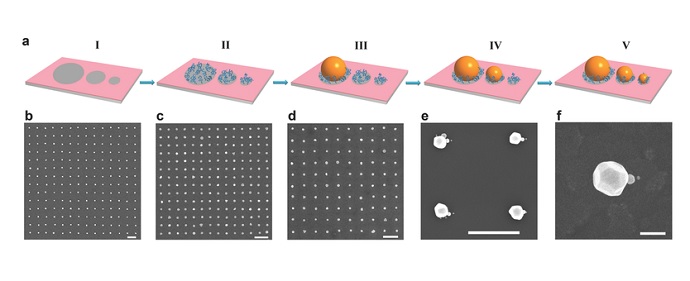
Deterministic Construction of Plasmonic Heterostructures in Well‐Organized Arrays for Nanophotonic Materials. Credit: Advanced Materials. Volume 27, Issue 45, pages 7314-7319, 14 OCT 2015 DOI: 10.1002/adma.201503336. http://onlinelibrary.wiley.com/doi/10.1002/adma.201503336/full#adma201503336-fig-0001

