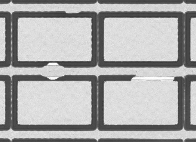
Elk Grove Village, IL, June 25, 2014 -- Sonoscan has announced its AW322 200™ fully automated system for ultrasonic inspection of MEMS wafers. Based on Sonoscan’s C-SAM® technology, the system images and identifies internal gap-type defects down to 5 microns in size. It is especially useful for finding non-bonds, voids and other defects in the seals surrounding the MEMS wafer cavities.
AW322 200™ system features include:
- Two loadports, two stages and multiple transducers, enabling it to image two 8-inch MEMS wafers simultaneously. Other models in the AW series are available to accommodate wafer sizes from 100-300mm.
- The SECS/GEM-enabled Robotic Handling Station includes alignment and drying operations.
- Waterfall™ technology to minimize water exposure during scanning.
- Sonoscan’s advanced analysis software for accurate application of the user’s accept/reject criteria.
In operation, the Robotic Handling Station counts and unloads wafers from the carriers, aligns wafers for scanning and positions wafers on the stage. The transducers travel over 1 m/s while pulsing ultrasound at frequencies up to 230 MHz and receiving thousands of return echoes per second. Both the transducers and the 500 MHz bandwidth pulser/receiver were designed and manufactured by Sonoscan.
The key defects imaged in MEMS wafers are non-bonds of the seal to a wafer, voids within the seal material and other gap-type defects that can compromise the hermeticity of the cavity.
After scanning, both the acoustic wafer image and the wafer data can be used for accept/reject determination. Criteria are defined by the user with respect to acceptable defect counts and sizes.
About Sonoscan®: Sonoscan is the leading developer and manufacturer of acoustic microscopes and sophisticated acoustic micro imaging systems, widely used for nondestructive analysis of defects in industrial products and semiconductor devices. For over 30 years, Sonoscan’s attention to customer needs and investment in R&D has created systems that set industry standards for speed and accuracy. Key products include C-SAM® systems for off-line and laboratory analysis and FACTS2™ for automated production inspection.

