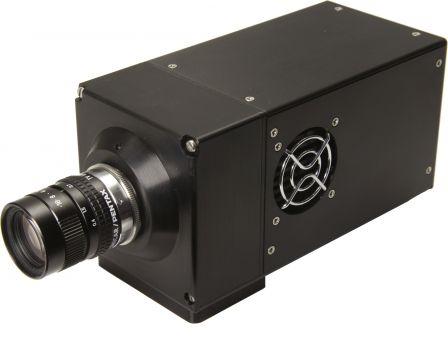
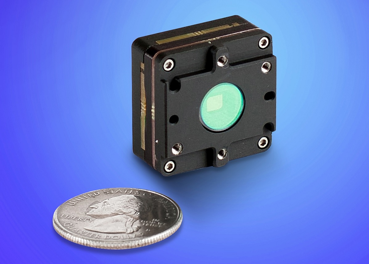
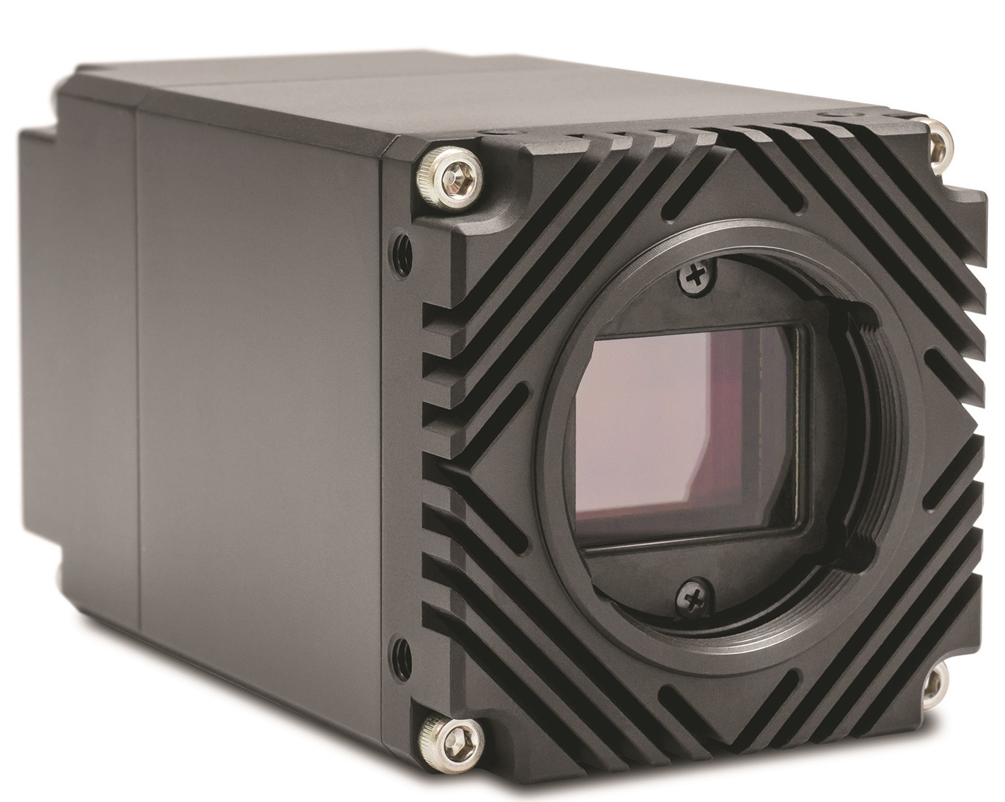
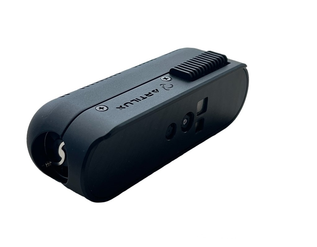
The camera is using selected InGaAs focal plane arrays with low dark current and low defective pixels.
Thanks to efficient cooling, stable offset and low dark current, the InGaAs camera allows reproducible acquisition for precise metrology measurements in the SWIR spectrum.
Camera link and Gigabit Ethernet Vision compliant interface enables easy integration into existing systems.
InGaAs sensors with visible extension are available in 640x512 resolution.
InGaAs sensors with SWIR extension are available in 320x256 resolution.
All cameras are available with passive cooling for:
• semiconductor inspection
• SWIR hand held vision enhancement
• SWIR airborne payload
Air cooling or water cooling are available for long exposure applications such as
• Astronomy
• Hyper spectral imaging
• Laser beam profiling
• Spectroscopy
Silicon wafer inspection with laser induced photoluminescence: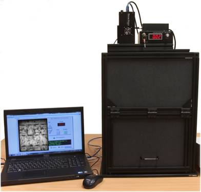
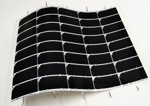
Solar cell / bare water photoluminescence inspection system
Photoluminescence (PL) performs non contact testing of PV cells and wafers by using a laser source. PL images are captured with a cooled InGaAs camera within 100ms exposure depending on source power used. PL imaging (proportional to minority carrier life time which correlates with cell efficiency) can be performed at any point of solar cell processing (bare wafer, wafer with oxide or nitride, patterned finished cell)
The on line testing solution is capable of very high throughput up to 3,600 wafers / cells per hour.
Intuitive software detects micro cracks, shunts, hot spots and low efficiency areas
• Bare wafer in line inspection
• Processed cell in line inspection
• Finished panel inspection (installed panels / prior to installation)
Application images 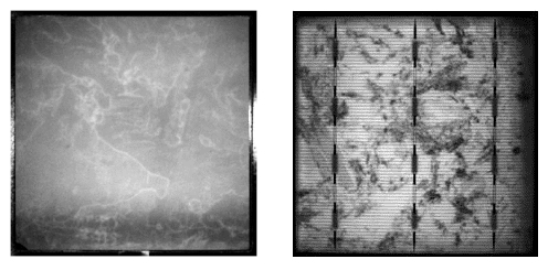
Silicon wafer photoluminescence (left). Solar cell photoluminescence (right)
For more information:

