05.01.2016
As part of their miniaturisation process, many of today's electronic components have already reached the nanometre size. One substantial factor contributing to successful functionality here is the ability to control electrical charges and fields on the atomic scale. A research team at Göttingen University has modelled a system that enables characterisation of the dynamics of single charge carriers within these electronic structures at molecular resolution. The results have been published in the scientific journal Nature Communications.
"The experiment consisted of a combination of optical excitation using a laser and scanning tunnelling microscopy," explains lead author Philipp Kloth at the 4th Physical Institute of Georg-August-Universität Göttingen. “Similar to a solar cell, excitation of the semiconductor surface by light generates free charge carriers." What is new is the role played by the scanning tunnelling microscope: It not only allows us to visualise the material on the atomic scale, but it can be additionally employed to inject charges into the system in a targeted manner. “This lets us actively drive the optically generated charge carriers out of equilibrium. The upshot is that the concentration of free charge carriers can be controlled, thereby enabling us to simulate the various screening mechanisms of electronic fields on the atomic scale," says co-author Dr. Martin Wenderoth, also at the 4th Physical Institute of Georg-August-Universität Göttingen.
These new results obtained by the Collaborative Research Centre (CRC) 1073 are prime examples of the recent developments accomplished within a new area of scientific focus at the Göttingen Campus. The CRC 1073 is concerned with gaining an understanding of how to control elementary energy conversion steps. Designed within the research project developed by Dr. Wenderoth in collaboration with Professors Claus Ropers and Alec Wodtke, the experiment represents a key building block in the investigation of such processes. “In future, we aim to employ the targeted use of optical excitation on surfaces to trigger the chemical processes of single molecules in order to then characterise them under the scanning tunnelling microscope," Dr. Wenderoth adds. This knowledge can help achieve a better understanding of the processes involved in the development of artificial photosynthesis and thereby contribute to evolving efficient applications for power production and energy conversion.
Original publication: Philipp Kloth et al. Controlling the screening process of a nanoscaled space charge region by minority carriers. Nature Communications. Doi: 10.1038/ncomms10108.
Interplay between electrical charges and light
Research team at Göttingen University discovers atomic-scale model system
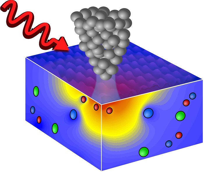
The nanometre-sharp tip of a scanning tunnelling microscope generates electrical fields at a semiconductor surface on the nanoscale. Optical excitation or carrier injection by tunnel current can actively drive the field screening to get out of equilibrium.


