August 27, 2014
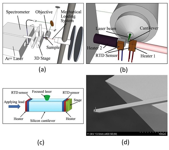
WEST LAFAYETTE, Ind. – A new research platform uses a laser to measure the "nanomechanical" properties of tiny structures undergoing stress and heating, an approach likely to yield insights to improve designs for microelectronics and batteries.
This new technique, called nanomechanical Raman spectroscopy, reveals information about how heating and the surface stress of microscale structures affect their mechanical properties. Researchers have discussed the merits of surface-stress influence on mechanical properties for decades. However, the nanomechanical Raman spectroscopy has offered the first such measurement, said Vikas Tomar, an associate professor in Purdue's School of Aeronautics and Astronautics.
Surface stress is similar to the surface tension that allows small insects to walk on water, makes water drops spherical, and causes human skin to initially resist a needle's penetration. On the relatively large scale of ordinary, everyday machines, surface stress is negligible, but it becomes critical for micro- and nanostructures, he said.
Recent findings are potentially important because silicon structures measured on the scale of micrometers and nanometers form essential components of semiconductor processors, sensors and an emerging class of miniscule machines called microelectromechanical systems.
"The functioning of such devices has been found to be highly affected by their operating temperature," Tomar said. "Such densely packaged devices generate considerable heat during operation. However, until now we have not been able to measure how heating and surface stress contribute to mechanical properties."
Information about the platform and new research findings were detailed in three papers published this year. The most recent appeared Aug. 15 in the Journal of Applied Physics. Tomar has led the research with former doctoral student Ming Gan, who has graduated and is now working in industry, and current doctoral student Yang Zhang.
In Raman spectroscopy, a laser interacts with the vibrating crystal lattice of materials, providing information about the chemical makeup of the materials.
"But we have not been able to incorporate in-situ stress or deformation into those chemical signatures," Tomar said. "Now we have combined nanomechanical measurements into Raman spectroscopy."
The researchers used the technique to study microscale silicon cantilevers, tiny diving-board shaped slivers about 7 microns thick, or roughly one-tenth the thickness of a human hair, and 225 microns long. The cantilevers were heated and stressed simultaneously. Surface stresses at the micro- and nanoscales were measured for the first time in conjunction with temperature change and a structure's deformation.
Findings show that heating a cantilever from 25 to 100 degrees Celsius while applying stress to the structure causes a dramatic increase in strain rate, or deformation.
The heating reduces bonding forces between atoms on the surface of the structures. The lower bonding force results in a "relaxed" state of the surface or near-surface atoms that progresses as the temperature increases, leading to cracks and device failure.
"The key is to be able to measure thermal and mechanical properties simultaneously because they are interrelated, and surface stress influences mechanical properties," Tomar said.
Findings are potentially important for the measurement of components in batteries to study stresses as they constantly expand and contract during charge-discharge cycles. Ordinary sensors are unable to withstand punishing conditions inside batteries.
However, because Raman spectroscopy uses a laser to conduct measurements, it does not have to be attached to the batteries, making possible a new type of sensor removed from the harsh conditions inside batteries.
"If you don't need onboard sensors you can go into extreme environments," he said. "You can learn how the stresses are evolving so that we can design better batteries."
Such a technology also could be important for development of super-strong composite materials that mimic those found in some marine animals that are able to survive in the extreme conditions found in ocean-floor hydrothermal vents. One obstacle is overcoming stresses that occur at the interfaces of different layers within the composite materials.
"These materials always break at the interfaces," Tomar said. "Now we can understand as the material is deforming how the interface stresses are developing, and this will allow us to predict how to modify them."
Purdue has filed a provisional patent for the new platform. The research has been funded by the National Science Foundation.
ABSTRACT
Surface stress variation as a function of applied compressive stress and temperature in microscale silicon
Ming Gan and Vikas Tomara
School of Aeronautics and Astronautics, Purdue University
Surface stress has been shown to affect the mechanical properties of materials at or below the microscale. Surface-stress-induced dislocation activity at such length scales has been shown to be a major factor affecting the mechanical behavior of materials. Defect generation as a function of applied stress at the microscale has previously been measured experimentally and predicted using simulations. However, the change in surface stress in a material in response to externally applied stress as a function of temperature has not been explored experimentally. Such an investigation is presented in this work for the case of microscale silicon samples. In-situ nondestructive measurements of the applied compressive stress and the corresponding microscale surface stress were performed from room temperature to 100 C. The applied stress was controlled by a nanomechanical loading system. Micro-Raman spectroscopy was used to measure the surface stress in-situ as the samples deformed under the applied uniaxial compressive stress. The surface stress was found to be lower than the applied stress at all temperatures. The difference between the surface stress and the applied stress became higher at higher temperatures indicating that surface relaxation was induced by the temperature increase. Based on the measured values and observed trends, an exponential Gaussian function is proposed to describe the stress as a function of surface depth. VC 2014 AIP Publishing LLC. [http://dx.doi.org/10.1063/1.4892623]

