September 18, 2014
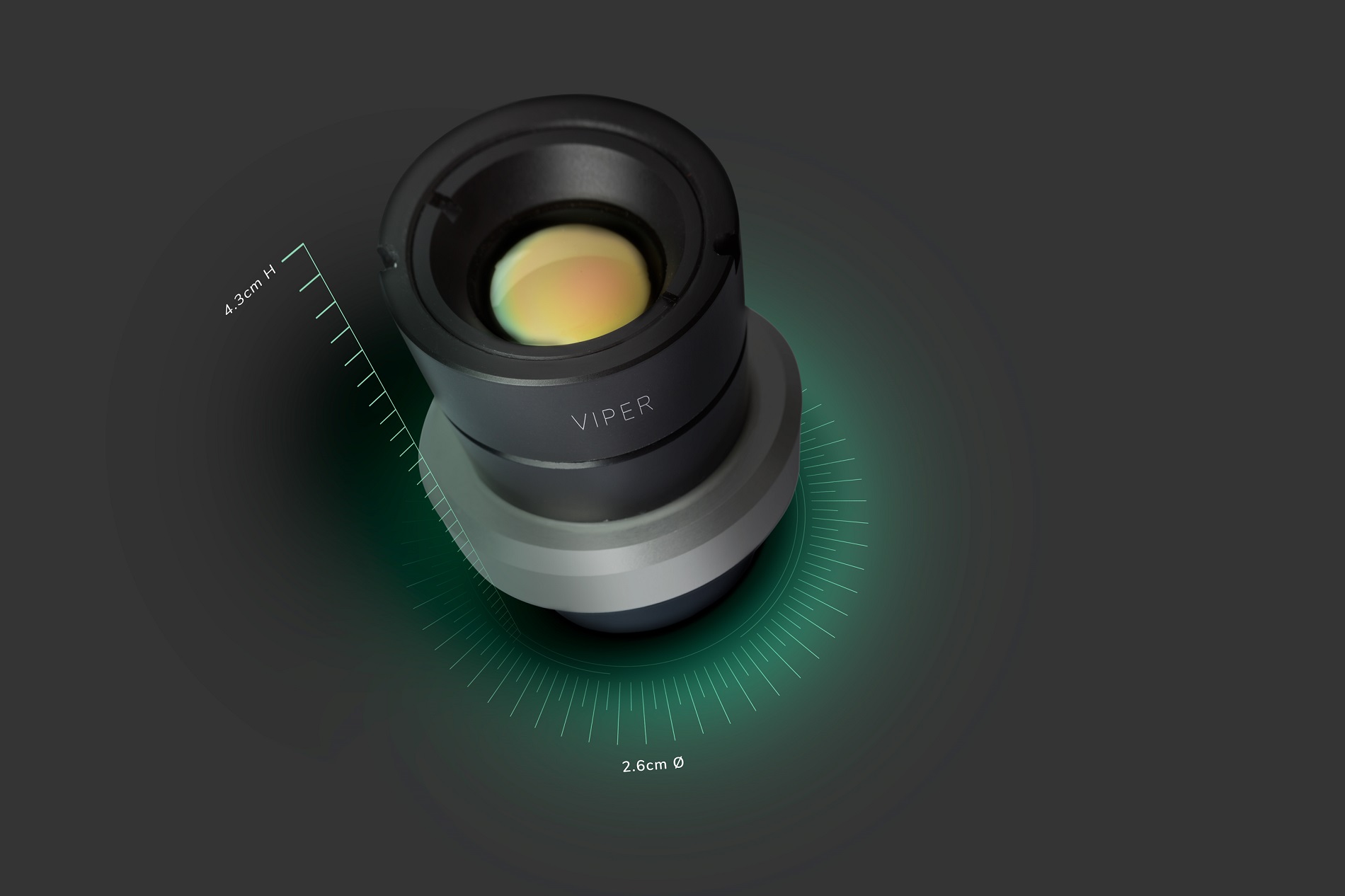
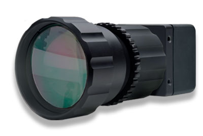
FAYETTEVILLE, Ark. – Engineering researchers at the University of Arkansas have fabricated a new semiconductor material -- germanium tin deposited in layers on a substrate of silicon -- that could be used to build better and less expensive infrared cameras for smartphones and vehicles.
“The performance of these simple structures indicates a promising future for germanium tin photodetectors,” said Fisher Yu, associate professor of electrical engineering. “The crystalline growth of these samples in a commercially available reactor allows for these infrared detectors to be available for expedient commercial implementation.”
Yu and colleagues Wei Du, postdoctoral fellow in the Department of Electrical Engineering; Benjamin Conley, doctoral student in the microelectronics-photonics graduate program; and Hameed Naseem, professor of electrical engineering, built devices using a process allowing thin films of germanium tin to be deposited on silicon, without damaging integrated circuits.
The researchers tested and measured the device at various percentages of material composition – 0.9, 3.2 and 7.0 – and at temperatures ranging from 77 to 300 on the Kelvin scale. Kelvin is a unit of thermodynamic temperature equal in magnitude to the degree Celsius. The researchers wanted to explore how the device would perform at room temperature for future night vision applications.
“This work will bring us much closer to the quality of images you find in military and satellite equipment,” Yu said.
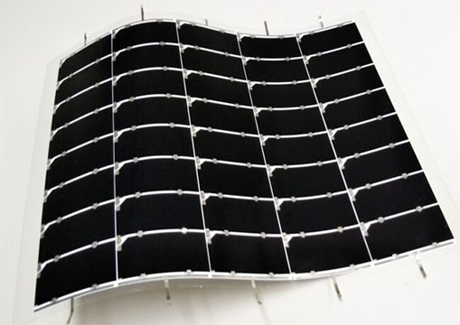
Only a few other research groups are working with germanium tin to produce semiconductor material for computer chips and electronics. The material has potential for other applications, including lasers and high efficiency solar cells.
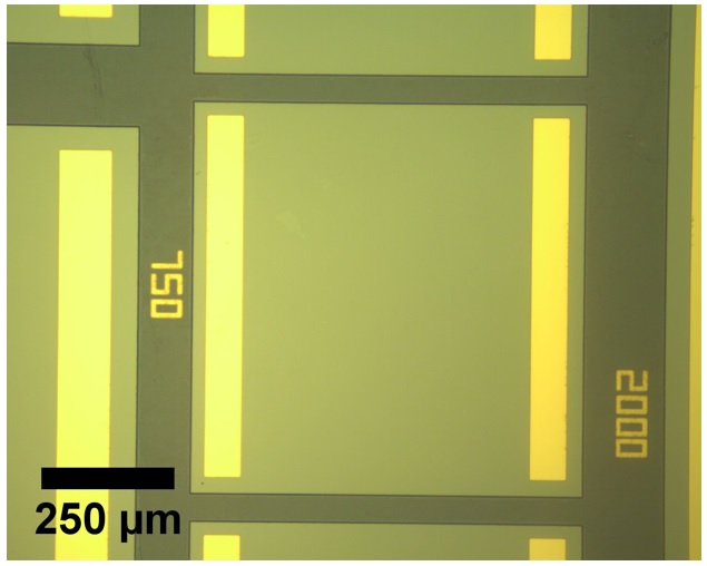
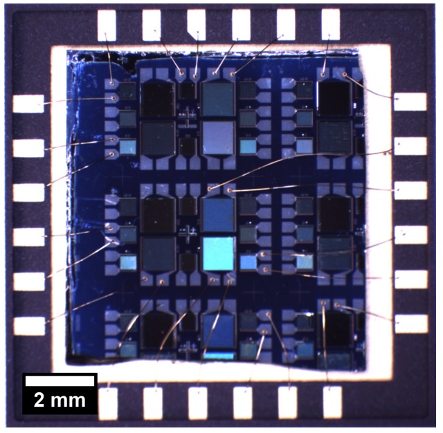
Figure 2. Ge1-xSnx photoconductors are fabricated as square mesas with gold contact pads. The entire device is coated with a thin layer (100 nm) of SiO2 for passivation.
The research group is collaborating with ASM International, a private company that builds most machine-epitaxy tools for fabricating microelectronics devices. The researchers have also started Arktonics, a research and development firm based in Arkansas, to investigate future commercialization of the materials and devices.
For this project, the researchers received funding from the National Science Foundation, the Army, the Air Force and the Defense Advanced Research Projects Agency. Their findings have been published in a recent issue of Optics Express, the international scientific journal of optics research.

