October 3, 2019
Tokyo, Japan — Sony Corporation announced today the forthcoming release of six new types of stacked CMOS image sensors with a global shutter function achieved using a back-illuminated pixel structure for industrial equipment applications.
These new sensors will be both compact and capable of high imaging performance without distortion of moving objects. They will employ Sony’s Pregius S — stacked CMOS image sensor technology, which comes with global shutter functionality made possible by Sony’s proprietary back-illuminated pixel structure, first announced in March 2019.
As automation and labor-saving measures are increasingly implemented in factories and logistics, machine vision cameras play an increasingly important role. The Sony's new image sensors target these applications, delivering both compactness and superior imaging performance, with higher precision and speed in recognition and measurement, thereby contributing to improved productivity and the "smartification" of industrial equipment.
To achieve advanced automation in factories and logistics by, for example, replacing conventional visual inspection with an automated process, it is necessary to improve inspection precision and efficiency by shortening inspection times. As such, machine vision cameras performing these functions require image sensors with higher resolution and faster speed than has been available so far.
Until now, increasing the number of pixels in image sensors to improve resolution has resulted in the downside of increased chip and camera size. However, if the pixel size is reduced to prevent increasing the camera size, then the light-accumulating area per pixel will correspondingly decrease, resulting in a drop in the sensitivity and saturation signal level. This results in image quality degradation, in turn leading to degradation in recognition and detection performance.
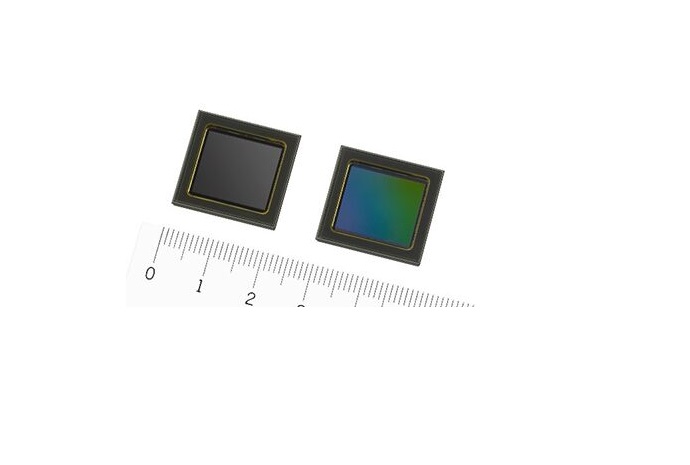
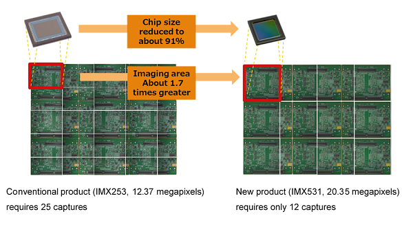
The new Sony sensor products provide a global shutter function enabling imaging without distorting moving objects. The proprietary back-illuminated pixel structure allows for a compact size of only 2.74µm square, which is about 63% of the conventional pixel area,*3 but still maintaining pixel characteristics such as sensitivity and saturation signal level. While using the same optical system as previous models, the number of pixels has been increased and the package size (area) has been reduced to about 91%.*3 This makes it possible to achieve a compact C-mount lens*4-compatible machine vision camera with higher resolution for improved inspection precision.
The new products achieve a readout frame rate approximately 2.4 times the speed of conventional image sensors*3 thanks to the highly flexible wiring layout of the back-illuminated pixel structure, and the use of the Scalable Low Voltage Signaling with Embedded Clock (SLVS-EC) high-speed interface standard developed by Sony. This results in shorter process time for measurements and inspections, contributing to significantly improved productivity.
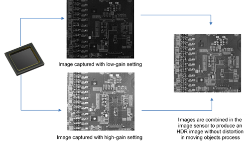
Further, the stacked structure allows for embedding various signal processing circuits such as the high dynamic range (HDR) processing circuit*5 that can prevent distortion in moving objects, thereby enabling myriad functions for various machine vision applications in a package more compact than conventional image sensors.
Main Features
CMOS image sensor equipped with global shutter function delivering both high definition and compactness
These new products achieve both compactness and high definition, plus distortion-free images of moving objects due to their stacked structures with the global shutter function made possible by the back-illuminated pixel structure. Sensitivity and saturation characteristics are maintained while achieving a size of only 2.74µm square, which is about 63% of conventional image sensors.*3 This allows for a resolution that is approximately 1.7 times higher than current standards for an optical system of the same size, with a package size reduced to about 91%*3 of conventional image sensors. This makes it possible to achieve a compact, 1.2-type high-resolution C-mount machine vision camera with 24.45 effective megapixels, enabling flexible installation in equipment and production lines.
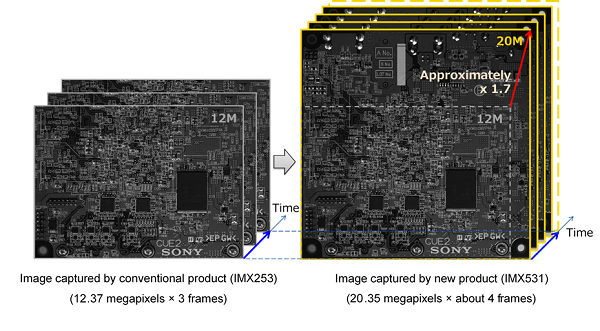
High definition allows for a larger imaging area, which in turn reduces the number of captures required
High-speed readout of image data
The back-illuminated pixel structure offers a high degree of freedom in wiring layout. Coupling this with SLVS-EC, an embedded clock*6 high-speed interface standard developed by Sony, produces a readout frame rate 2.4 times faster than conventional image sensors.*3 This makes it possible to shorten takt time of production equipment and devices, and to improve throughput.
Sony is providing an expansive lineup, including the high-speed IMX530/531/532 models for high-end cameras using high-speed bandwidth, in addition to the standard IMX540/541/542 models that support 5G bps supplementing the expansion in the application of USB 3.0 and 5GigE. These diverse products will contribute significantly to productivity improvements such as reducing the time needed for measurement and inspection processes for various applications, including inspection, image recognition, identification, and measurement.
High-speed readout shortens time required for inspection processes
Realization of high functionality to improve usability
The stacked structure makes it possible to mount various signal processing circuits, allowing for a CMOS image sensor that is both compact and highly functional. By arranging the signal circuits in a stacked configuration, it is possible to achieve many functions in a package that is more compact than conventional image sensors.*3 These include data optimization functions (ROI, self-trigger, etc.) that extract only the information needed from the image data, new features such as internal HDR processing using dual A/D converters preventing distortion in moving objects, and short interval exposure control, thereby responding to various needs in diversifying machine vision applications.
*1: Based on image sensor effective pixel specification method.
*2: The dates given for sample shipment date (planned) are for the black and white model samples. Color model samples will be available for shipment one month later.
*3: Comparison between Sony's IMX253 and IMX531 CMOS image sensors (1.1 type, 12.37 effective megapixels)
*4: An industry standard mount for joining the lens and camera body.
*5: Installed in the IMX530/531/532.
*6: In this method, the clock signal is embedded in the data transmitted. Since there is no need to address skew between lanes, the method is suited to high-speed transmission and simplifies the board design.
*7: Converted value using 1Digit = 0.2445 mV (during 12 bit output), 1Digit = 0.9779 mV (during 10 bit output), 1Digit = 0.9779 mV (during 8 bit output).
Source: