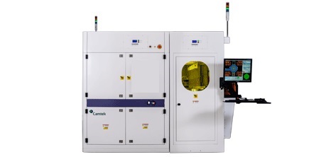
MIGDAL HAEMEK, Israel – June 22, 2016 – Camtek Ltd. (NASDAQ: CAMT; TASE: CAMT), today announced the launch of an innovative inspection method for Fan-Out Wafer Level Packaging (FOWLP). This new inspection method compares the image acquisition of the dies on the reconstructed wafer with the computer-aided design (CAD) data used in fabricating the wafer.
Ramy Langer, Vice President and Head of Camtek's Semiconductor Division, commented, “Camtek has more than 25 years of experience working with CAD data in our Automated Optical Inspection (AOI) systems for the PCB industry. The development of this new method for the inspection of Fan-Out applications is based on this experience and accumulated know-how.”
Continued Mr. Langer: “Industry experts expect Fan-out wafer level packaging technology to grow in excess of 30% annually over the coming years. The Fan-out packaging process imposes many inspection challenges, especially due to alignment issues. We believe that using the CAD as a reference for detecting the reconstructed wafers will make our Eagle product the tool of choice for Fan-out applications.”
ABOUT CAMTEK LTD.
Camtek Ltd. provides automated and technologically advanced solutions dedicated to enhancing production processes, increasing products yield and reliability, enabling and supporting customer’s latest technologies in the Semiconductors, Printed Circuit Boards (PCB) and IC Substrates industries.
Camtek addresses the specific needs of these interconnected industries with dedicated solutions based on a wide and advanced platform of technologies including intelligent imaging, image processing and functional 3D inkjet printing.