JENA, OBERKOCHEN/Germany – February 20, 2014.
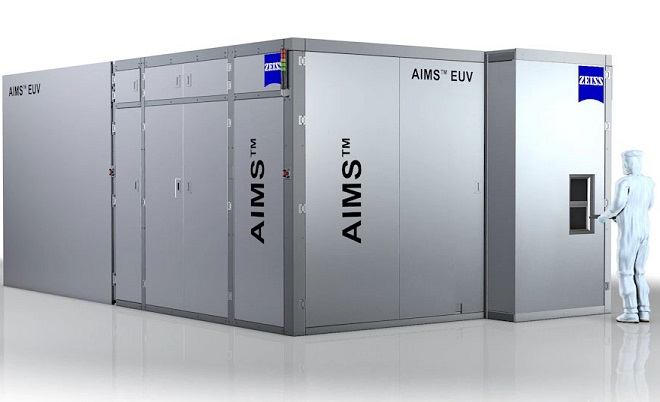
The Semiconductor Manufacturing Technology business group of ZEISS made significant progress in the development of the actinic aerial image metrology system AIMS™ EUV. First images of EUV photomasks were taken by the prototype of the system.
"The first images are a major milestone, because they verify the concept and the design of the whole system. We produced evidence that not only the optics is well defined, but also the source as well as all other major components are working together," states Dr. Jan Hendrik Peters, EUV Program Manager of Carl Zeiss SMS GmbH.
The AIMS™ EUV platform represents an essential tool for the development and manufacturing of defect-free EUVL masks supporting the 16 nm half-pitch (HP) technology node requirements with extendibility to the 11 nm HP node. Consequently the development of this tool is part of the EUVL Mask Infrastructure (EMI) Consortium activities. SEMATECH launched EMI in 2010 to address key infrastructure gaps for EUV in the area of mask metrology, by funding development of critical metrology tools.
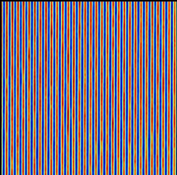
First Aerial Images taken on 64nm photomask structures, corresponding to 16nm at wafer level.
“The AIMS™ EUV tool will be one of the most precise optical instruments fabricated for the semiconductor industry, and the EMI members are pleased to see our collaboration facilitate this technical accomplishment. With first images now available ZEISS is showing significant progress in building a production ready tool. Mask defectivity remains a key challenges to EUV readiness and it is exciting to see AIMS™ continue its journey towards realization," comments Michael Goldstein, EMI Program Manager & Sr. Principal Physicist, Intel assignee at SEMATECH.
The resolution of the system is already excellent and achieves the specification of the AIMS™ EUV system. The first images were taken on 64nm mask structures, corresponding to 16nm half-pitch at wafer level. In the course of the year the first customer masks will be measured on the system.
In parallel the preparations for the complementary AIMS™ EUV infrastructure is ongoing. Beginning in 2013 the first AIMS™ EUV Field Service Engineers were trained for installing and servicing the systems in the field.
Further Information
Carl Zeiss SMT