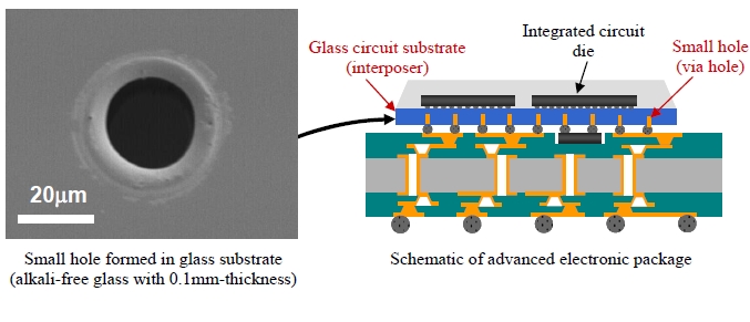
TOKYO, February 13, 2014- Mitsubishi Electric Corporation (TOKYO: 6503) announced today it has developed micro glass-processing technologies that use a pulsed CO2 laser to drill the world's smallest holes measuring just 25 microns in diameter (1 micron equals 1/1,000 millimeter) in glass substrate. The technology is expected to enhance the use of glass circuit substrates for the improved performance of electronic devices.
A far-infrared CO2 laser with a wavelength of about 10 microns is used to drill transparent glass. Short laser pulses lasting 1/1,000,000th of a second can reduce heating of the glass substrate during the drilling. Surface treatment technology is applied to suppress the over-enlargement of drilled holes. Some 200 holes per second can be drilled using a high precision, high-speed galvano mirror to scan the laser beam. CO2 lasers, which can easily be geared to high-power, are used widely in industry and offer vastly improved productivity compared to conventional ultraviolet laser oscillators characterized by high cost and limited light-harvesting properties.