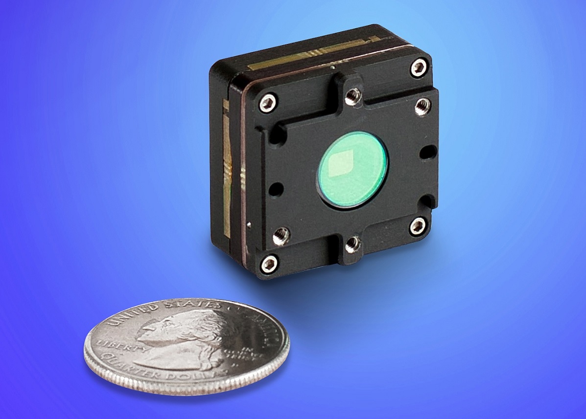
Stuttgart (Germany), November 5, 2018 — This week at Vision 2018 (November 6-8 2018), imec, the world-leading research and innovation hub in nanoelectronics and digital technologies, presents a high-speed UV-sensitive time-delay-integration (TDI) imager that is based on charge-coupled-device (CCD)-in-CMOS technology. The TDI imager has a quantum efficiency of more than 70% in the (near-)ultraviolet (UV) region, making it an appropriate tool for industrial machine vision, in particular inspection in semiconductor manufacturing processes. The specialty imager broadens imec’s CCD-in-CMOS-based TDI imager portfolio, that is offered through various business models – ranging from full-custom design to evaluation cameras.
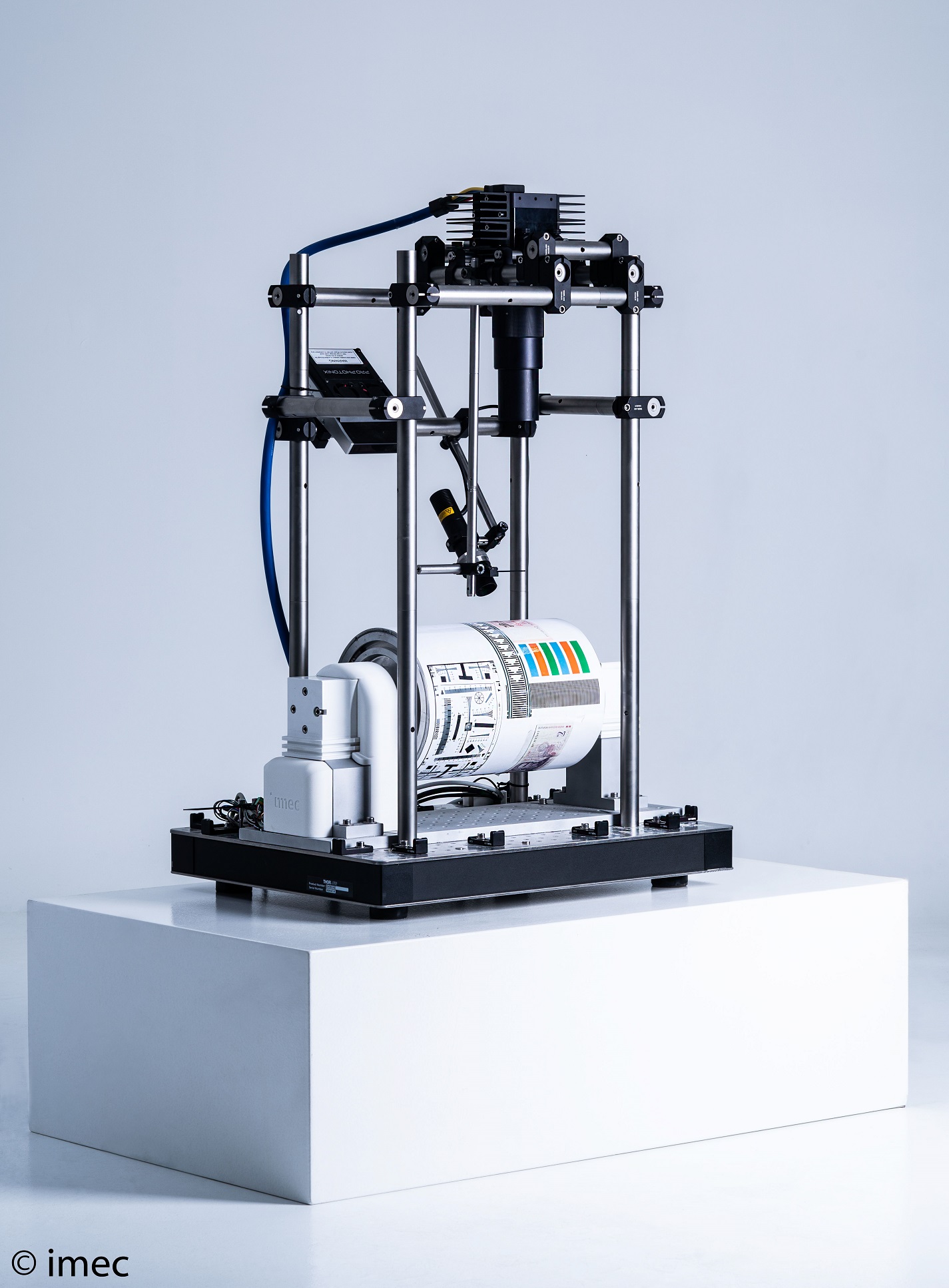
The new imager was fabricated using imec’s TDI CCD-in-CMOS technology, that combines CCD TDI pixels and CMOS readout in one technology. This combination allows the best of both worlds to be realized on a single line-scanning imager: low-noise, highly sensitive TDI performance, and low-power, on-chip integration of fast and complex readout circuitry.
UV sensitivity is obtained by applying imec’s backside illumination technology in combination with a dedicated antireflection coating. With backside illumination, light directly enters the imager from the backside, significantly enhancing the quantum efficiency of the image sensor. By adding a UV-specific antireflection coating, a high peak quantum efficiency of more than 70% is reached in the (near-)UV region of 250 – 400nm. Being sensitive to wavelengths smaller than the visible allows the imager to detect very small features – making the technology in particular attractive for semiconductor inspection applications, such as mask, wafer and particle inspection.
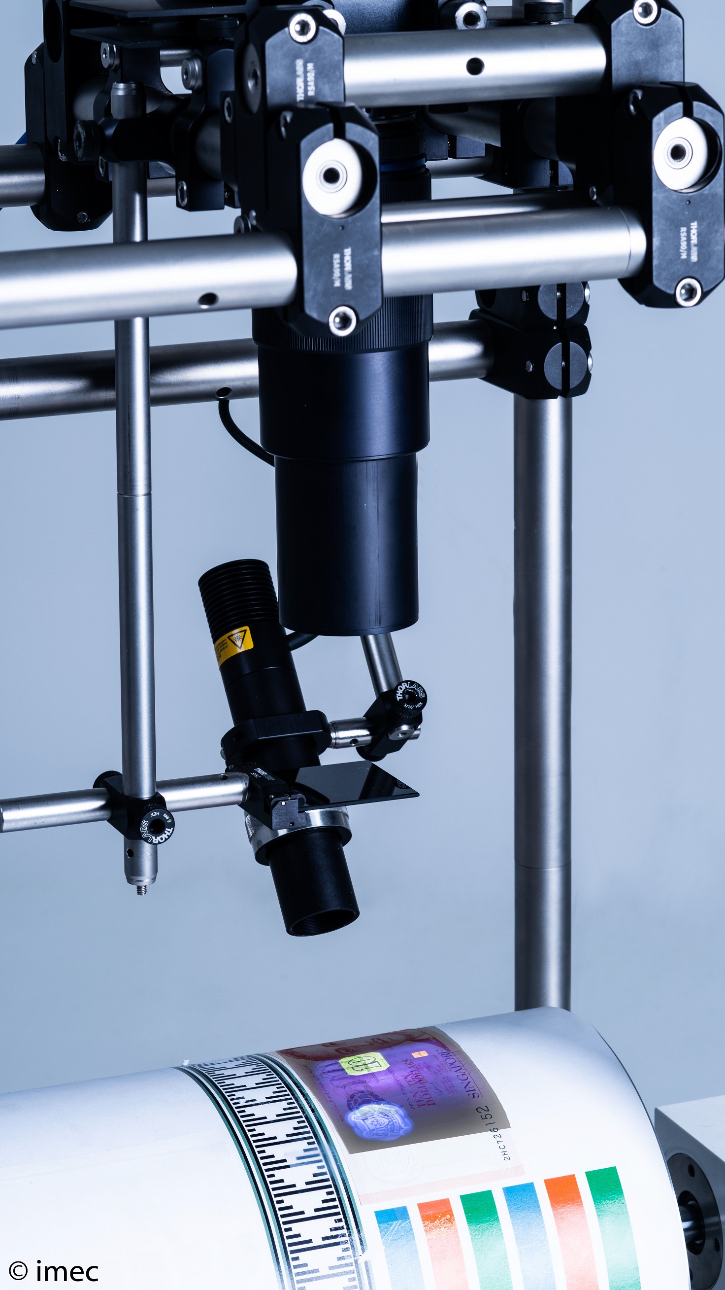
The TDI sensors are manufactured on 200mm wafers by using imec’s CCD process module inside its 130nm CMOS process flow. This cost-effective manufacturing flow is compatible with other wafer-level post-processing techniques such as spectral filter integration for enhanced TDI performance. The resulting image sensors have a high sensitivity and speed (up to 300kHz line rate)and have a low power consumption.
Maarten Rosmeulen, program manager image sensors at imec: “With this high-speed, low-power TDI imager, we are happy to expand our range of TDI CCD-in-CMOS image sensors with UV sensing capabilities. We can now offer TDI CCD-in-CMOS image sensors with high quantum efficiencies in both the UV and visible ranges, enabling a wealth of high-end applications, including remote sensing, medical imaging and industrial machine vision.”
More information at: