May 17, 2017
“The laser is a solution seeking a problem,” said Ted Maiman in 1964. Today, the laser has proven the best solution to an array of problems. At LASER World of PHOTONICS 2017 in Munich/Germany, the Fraunhofer Institute for Laser Technology ILT will be demonstrating how it is using process technology to enable efficient laser applications in a range of sectors, thereby driving forward Digital Photonic Production in the 21st century.
Over the past decades, new beam sources have taken the laser community by storm, with disk, fiber and diode lasers all making the transition into industrial manufacturing – and now ultrafast lasers, too.
“With the most powerful lasers, it’s a case of working out how to bring that power to bear,” says Dr. Arnold Gillner of the Fraunhofer ILT in Aachen. “Right now, we need a thorough understanding of the processes at work and the right process technology if we are to open up new fields of application for the laser.”
This is precisely what Fraunhofer ILT in Aachen is working on, in addition to its research of a range of beam sources. The focus of R&D activities is not only on efficiently distributing the laser beam, but in the first instance on developing a thorough process understanding – which can then be used to optimize whole machines and systems from simulation to full-scale production.
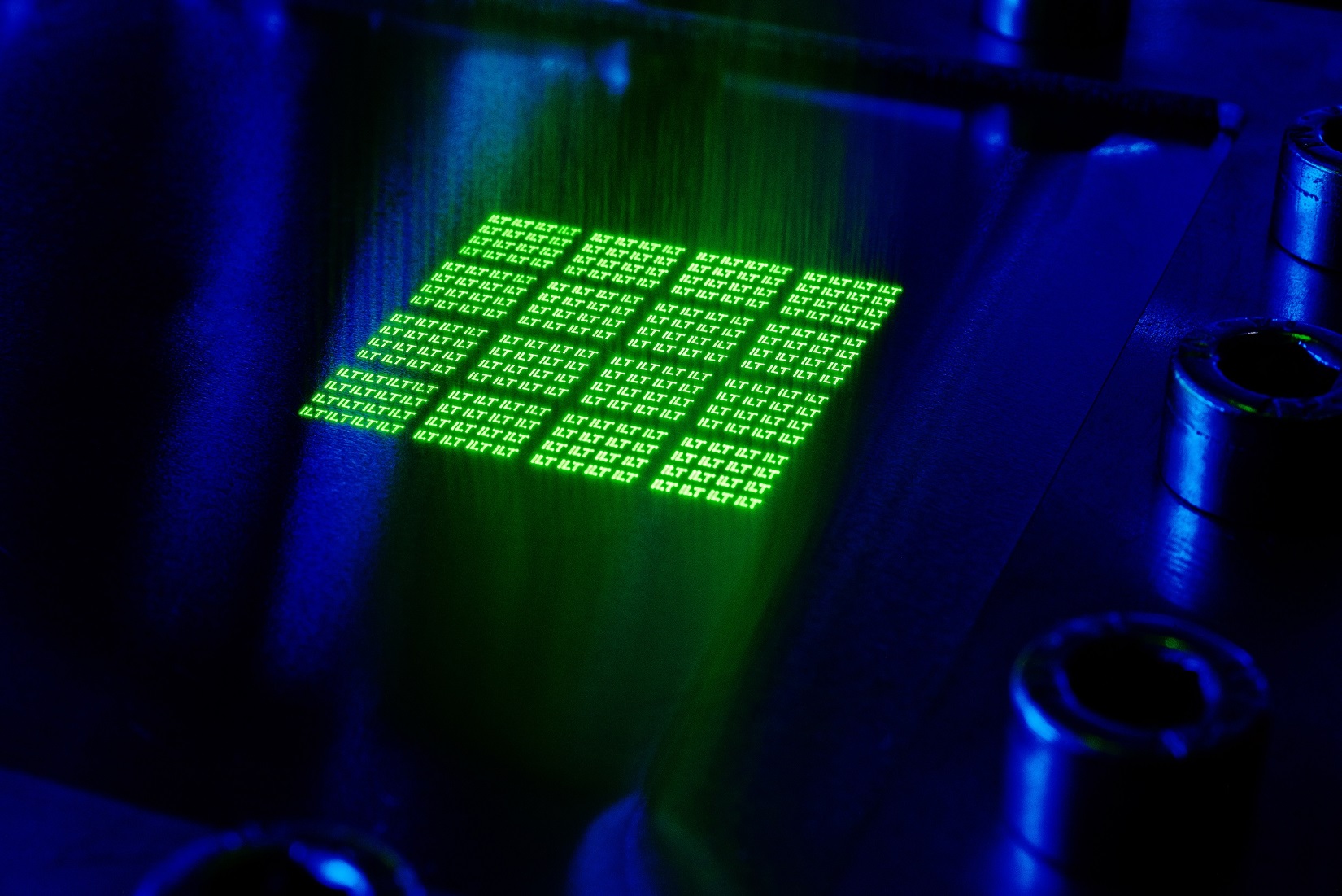
Increasing productivity is currently the biggest issue with USP lasers. Multiple beam systems offer a possible solution.
© Photo Fraunhofer ILT, Aachen, Germany / V. Lannert
Laser Material Deposition Takes off
A deep understanding of the processes at work is at the heart of a new technique known as extreme high-speed Laser Material Deposition (known by its German acronym EHLA). Thomas Schopphoven explains the key element of the new process: “With EHLA, the laser melts the powder particles while they are still above the weld pool.” As a result, components can be coated 100 to 250 times faster than with conventional laser material deposition, with a minimum of heating.
The technique is intended to enable surfaces to be coated rapidly, offering a resource-efficient and cost-effective way of applying thin coats just tenths of millimeters thick. These coatings do not chip, unlike hard chrome plating, and the EHLA process is also more environmentally friendly.
Applying Microstructures over Large Areas Using Ultrashort Pulses
Lasers have long been used in the automotive industry for cutting and welding tasks. Now they have a new task: the application of microstructures to injection molds over large areas. Microstructures can be found all over the car, for instance in the cylinder, where they reduce fuel consumption, and in the panels of the interior, where they assure a high-quality finish.
Lasers with ultrashort pulses are very effective at applying these structures up to the micrometer range, but are let down by their pace. Experts in Aachen have come up with an elegant solution to the problem by combining two beam sources: a picosecond laser for the finest work, and a fast nanosecond laser for larger areas.
Known as eVerest, the project is sponsored by the German Federal Ministry of Education and Research, and aims to develop complete machine and system technology for the technique. This simpler solution would eliminate complex etching processes, and even pave the way for automation in a significant part of the process.
The Future is Digital
The laser industry is also looking more and more to Industry 4.0. In the future, industrial laser users will be seeking to fully exploit all their production process data.
In Aachen, systematic development of digitally connected laser production is in full swing in the form of the “Research Campus Digital Photonic Production” sponsored by the German Federal Ministry of Education and Research.
At LASER World of PHOTONICS 2017, to be held in Munich/Germany June 26-29, experts from the Photonics Cluster at the RWTH Aachen Campus will be demonstrating how they are already collaborating with numerous companies to shape the future of Digital Photonic Production.
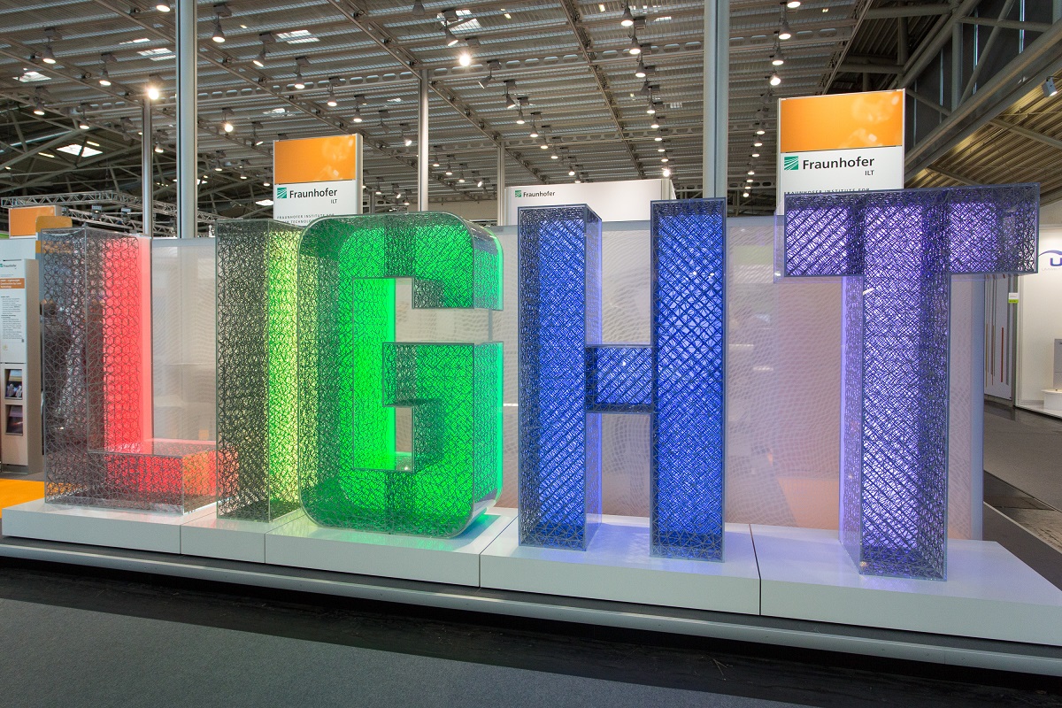
Fraunhofer ILT Stand at the LASER World of PHOTONICS 2015: The 3D-printed six-foot »LIGHT«-letters refer to the Additive Manufacturing and Laser Processes for Lightweight-Construction of the experts from Aachen
© Photo Fraunhofer ILT, Aachen, Germany / Klaus D. Wolf
Fraunhofer ILT at LASER 2017
At the joint Fraunhofer stand, A2.431, the experts from Aachen will be showcasing a range of new developments. These include the MERLIN project, for which they will be presenting a laser system for the measurement of methane concentrations in the atmosphere using satellites.
Also on show will be a new 3D printer for metal components. Offering a highly cost-effective model and a comprehensive range of consultancy services, the Aachen researchers will be targeting SMEs looking for a no-nonsense way to build up their expertise in additive manufacturing (in this instance, Selective Laser Melting in particular).
At the LASER World of PHOTONICS practice-oriented application panels, our experts will be present with numerous lectures.
A list of the ILT-speakers and further information about the trade fair can be found at the ILT event-website: LASER World of PHOTONICS

