02-16-2016
SCHOTT, the international technology group and specialty glass expert, will debut the significantly improved photo-sensitive glass FOTURAN® II, which highlights the company’s expanded thin glass and wafer portfolio, at SPIE Photonics West. This material is characterized by advanced photosensitivity and homogeneity. These unique properties combined allow a high aspect ratio, and therefore enable radio frequency (RF) components and microelectromechanical systems (MEMS) manufacturers to create substrates with significantly finer structures for various applications. SCHOTT will present FOTURAN® II wafers for the first time at SPIE Photonics West (booth #1314) from Feb. 16 to 18, in San Francisco.
SCHOTT is a pioneer in photosensitive glass. For over 30 years, the company’s FOTURAN® glass has been a well-known and proven specialty glass material whenever extremely fine structures are needed without the efforts of regular resist-based photolithography. FOTURAN® is a proven technology in various application fields in micro-systems technology, semiconductors, telecommunications, RF components, microfluidics, micro-optics, and MEMS sensors.
For example, structured substrates out of the improved FOTURAN® II allow for power inductors with a small footprint in high frequency RF devices, a high Q factor, and high self-resonance frequency (SRF). In the field of biotechnology, microfluidics is moving to the mainstream, aiding a wide variety of fields including medical diagnostics, life sciences research, and drug delivery and synthesis. Here, FOTURAN® II can be used to produce re-usable, easy-to-clean, and optically transparent titer-plates. In contrast to silicon sensors, FOTURAN® II’s structurability enables the design of flow sensors with small thermal masses, creating ultra-fast response times and very good chemical stability. Lastly, FOTURAN® II can be used in semiconductor substrate and packaging processing on standard equipment.
Enhanced manufacturing leads to improved benefits
FOTURAN® II’s improved production process ensures high reproducibility and homogeneity of photosensitivity and optical characteristics across the wafer.
“The special properties of FOTURAN® II enable research and industry experts to create substrates with significantly finer microstructure sizes at the micrometer level with unprecedented aspect ratios,” explains Fredrik Prince, Head of the Strategic Business Field Thin Glass & Wafers. “These characteristics allow engineers to pack more power into devices ranging from semiconductors to medical equipment, and pushes the technology smaller and smaller without sacrificing performance.”
FOTURAN® II is available in 6- or 8-inch round wafers and square substrates up to 200 x 200 mm with thicknesses between 0.5 mm and 1 mm. The wafers are structured and processed in three steps: UV-exposure (with standard lithography equipment without the use of photo-resist), tempering (heat treatment), and etching; additional ceramization is also an option when even higher temperature stability is required.
Further information: http://www.us.schott.com/advanced_optics/english/products/optical-materials/thin-glass/foturan-2/index.html
FOTURAN® is a registered trademark of SCHOTT AG.
SCHOTT to Introduce FOTURAN® II Glass Wafer at Photonics West
Improved photo-structurable glass ideal for RF/MEMS and biotech applications
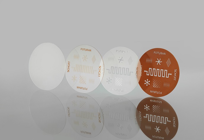
SCHOTT’s photo-sensitive FOTURAN® II glass wafers can be structured and processed in three steps: UV-exposure, tempering, etching, and optionally ceramization. Photo: SCHOTT


