06 Jan 2016
written by Miss Amy Sutton
Research published today in Nature’s Scientific Reports demonstrates carbon nanotubes creating wafer-thin, flat structures that enable the miniaturisation of a range of optical devices. Removing the need for traditional curved refracting lensing systems, which are generally bulky and expensive, will enable new compact optical systems based on this nanotechnology.
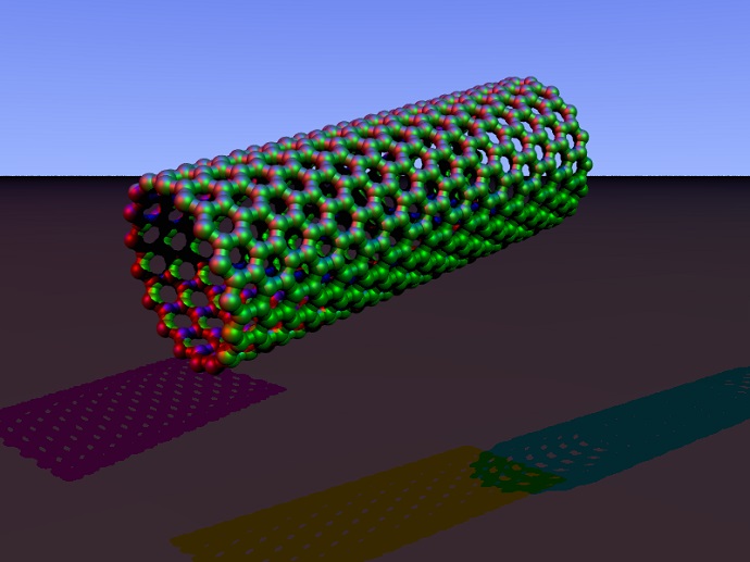
A team of researchers from the University of Surrey’s Advanced Technology Institute (ATI) grew vertically aligned carbon nanotubes, in a grid-like formation on glass. The material is either highly transparent or opaque depending on its angle with respect to the beam. This property makes it ideal for either collimating a beam of visible white light; or for absorbing stray light that is off the axis of the carbon nanotubes. This enables significant improvement to line-of-sight applications such as optical data transfer, or the rejection of stray light in high specification space telescopes.
Lead author of the work, James Clark from the Advanced Technology Institute explained, “One approach to realising compact optical systems, which is an alternative to that used here, is a Veselago lens which is made from artificial ‘metamaterials’. However, currently the obstacles in translating this theory to practical use are numerous.”
Professor Ravi Silva, Director of the ATI, and co-author of the work noted: “Collimation maintains an accurate record of the image and is classically done by using two lenses, each with a specific shape and placed a certain distance from each other. What we have shown in this study is that carbon nanotubes grown in this way can produce a well-collimated beam of visible light using a single flat material, a practical feature of a Veselago lens. This will lead to a new approach to small and flexible optical devices.”
The next step for this work is to incorporate this material into existing technology. The ATI has already demonstrated low-temperature growth processes to enable direct wafer-scale integration of vertical CNTs with CMOS devices.


