June 06, 2013
Optical spectroscopic imaging has taken a leap into the intramolecular regime with an approach that achieves subnanometre spatial resolution. The technique should find applications in photochemistry and nanotechnology.
The goal of optical microscopy is to visualize the physical and chemical properties of objects too small to be seen with the naked eye. However, objects separated by less than approximately half the wavelength of the light that is used to illuminate them can in general not be distinguished, owing to the inherent wave nature of light. The development of near-field optics has broken this spatial-resolution limit and has enabled optical imaging and spectroscopy with a resolution of a few nanometres. On page 82 of this issue(Jun 6th), Zhang et al.1 report an optical spectroscopic imaging approach that achieves subnanometre resolution and resolves the internal structure of a single molecule.
In 1928, Edward Hutchinson Synge came up with an idea for nanometre-scale optical microscopy2, possibly inspired by Richard Zsigmondy’s ultramicroscope3. Synge suggested that light scattered by a small particle placed close to an object could act as a localized light source. Spatial resolution would then be determined by the size of the particle rather than the wavelength of the light used.
The experimental implementation of this idea, however, had to await the invention of scanning tunnelling microscopy (STM) in the 1980s, because of the need for precise, nanometre-scale spatial control of the sample and scatterer. STM, which is based on a quantum tunnelling current of electrons between a nanoscale tip and the sample, provided spatial resolution down to the atomic scale4. This breakthrough was followed by the development of atomic force microscopy (AFM). Because AFM does not rely on a tunnelling current, it can be used on a much wider range of samples, including non-conducting materials and soft matter.
Although STM, AFM and other techniques such as transmission electron microscopy and X-ray microscopy can achieve results with atomic resolution, the goal of reaching this ultrahigh resolution, in combination with the detailed and sensitive information that optical spectroscopy would provide, remained unachieved. The power of optical spectroscopy lies in its sensitivity to energetic details of the configuration and electronic structure of atoms and molecules in solids, and the way in which these fundamental properties are coupled. In particular, when probing vibrational motion between atoms, optical spectroscopy can be used to identify the chemical constituents of molecules and solids.
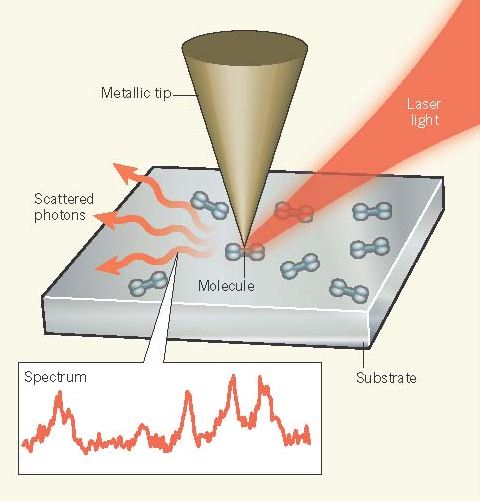
Possible ways of combining STM and AFM with optical techniquesto provide nanometre-scale spectroscopic information have been extensively explored. The initial approach of near-field scanning optical microscopy (NSOM), which is based on the use of a tapered fibre with an STM or AFM feedback mechanism for controlling the sample–tip distance on the nanometre scale, provided5 spatialresolution to below 100 nm. Other methods that paved the way to higher resolution and greater versatility included scanning plasmon near-field microscopy6 and photonic force microscopy7.These developments led to the technique of scattering scanning near-field optical microscopy (s-SNOM). This generalization of NSOM and the early methods provides the most versatile realization of Synge’s vision8. In s-SNOM, the apex of the tip (preferably metallic) serves as the nanoscale scatterer, enabling almost any optical spectroscopy technique to be extended to near-field use for probing electronic and vibrational properties with a spatial resolution of 10 nm or better9,10. (Following the development of near-field microscopy, powerful, super-resolution far-field optical microscopic techniques emerged, but these have typically provided limited spectroscopic information.)
Meanwhile, STM has been extended to yield vibrational and thus chemical spectroscopic information with atomic resolution using an approach called inelastic tunnelling spectroscopy11. Although so far limited to operating at cryogenic temperature conditions, this technique set the stage for what is possible in terms of spatial resolution and spectral content.
Zhang et al. extend these previous efforts by combining low-temperature STM (78 kelvin) in an ultrahigh vacuum with Raman spectroscopy as an optical vibrational spectroscopy technique (Fig. 1). In Raman spectroscopy, incident laserphotons lose energy to specific molecular vibrational excitations in the sample, thus providing chemical ‘fingerprints’. The combination of Raman spectroscopy with specially designed silver or gold STM tips, which can confine and locally enhance the incident laser field at the apex, is called tip-enhanced Raman scattering (TERS). Using STM and silver tips, Zhang and colleagues achieved subnanometre spatial resolution and were able to map spectroscopic signatures inside a single molecule, and to determine how these signatures changed with molecular orientation.
Optical spectroscopy with atomic-scale spatial resolution previously seemed impossible, with s-SNOM and TERSthought to be limited by the depth to which light can penetrate into the metallic tip— on the order of 10 nm at visible and infrared wavelengths. However, optical fields can be confined to almost arbitrarily small regions12, which are limited only by the size at which the electrons in a homogeneous medium cease to behave as free particles. This limit is given by the Thomas–Fermi screening length of about 0.1 nm, below which non-local effects become significant. The fact that scanning near-field optical microscopy techniques have not previously achieved such high spatial resolution is probably due to the AFM and STM instruments used for optical techniques not having been designed with atomic resolution in mind.
The mechanisticdetails underlying the unprecedented optical resolution and molecular sensitivity obtained in Zhang and colleagues’ work is not yet completely clear. The TERS signal measured seems to increase nonlinearly with increasing power of the incident laser, in contrast to what is observed with conventional Raman or TERS spectroscopy. The authors attribute this to a higher-order nonlinear response generating the signal. Moreover, the TERS signal was found to be sensitive to the optical properties of the tip in unexpected ways. The combination of these factors raises questions for theory and calls for further investigation.
The authors’ work opens up avenues for probing and even controlling materials on molecular scales. Because it can be combined with essentially any optical technique, detailed specific chemical and physical information about many kinds of samples can be obtained, with the only limitation being the requirement of STM for an electrically conductingsample. The highly localized laser-field enhancementcan also be used for photochemistry on the nanoscale, making and breaking bonds on the molecular level. Ultimately, this development could lead to new techniques for probing and controlling nanoscale structure, dynamics, mechanics and chemistry.
Source: Nature
Joanna M. Atkin and Markus B. Raschke (Department of Physics, Department of Chemistry, and JILA, University of Colorado at Boulder, Boulder, Colorado 80309-0390, USA.)
1. Zhang, R. et al. Nature 498, 82–86 (2013).
2. Synge, E. H. Phil. Mag. 6, 356–362 (1928).
3. Siedentopf, H. & Zsigmondy, R. Ann. Phys. 315, 1–39 (1902).
4. Binnig, G., Rohrer, H., Gerber, C. & Weibel, E. Phys. Rev. Lett. 50, 120–123 (1983).
5. Pohl, D. W., Denk, W. & Lanz, M. Appl. Phys. Lett. 44, 651–653 (1984).
6. Specht, M., Pedarnig, J. D., Heckl, W. M. & Hänsch, T. W. Phys. Rev. Lett. 68, 476–479 (1992).
7. Florin, E.-L., Pralle, A., Hörber, J. K. H. & Stelzer, E. H. K. J. Struct. Biol. 119, 202–211 (1997).
8. Atkin, J. M., Berweger, S., Jones, A. C. & Raschke, M. B. Adv. Phys. 61, 745–842 (2012).
9. Cialla, D. et al. J. Raman Spectrosc. 40, 240–243 (2009).
10.Yano, T., Verma, P., Saito, Y., Ichimura, T. & Kawata, S. Nature Photon. 3, 473–477 (2009).
11.Stipe, B. C., Rezaei, M. A. & Ho, W. Science 280, 1732–1735 (1998).
12.Kreibig, U. & Vollmer, M. Optical Properties of Metal Clusters (Springer, 1995).


