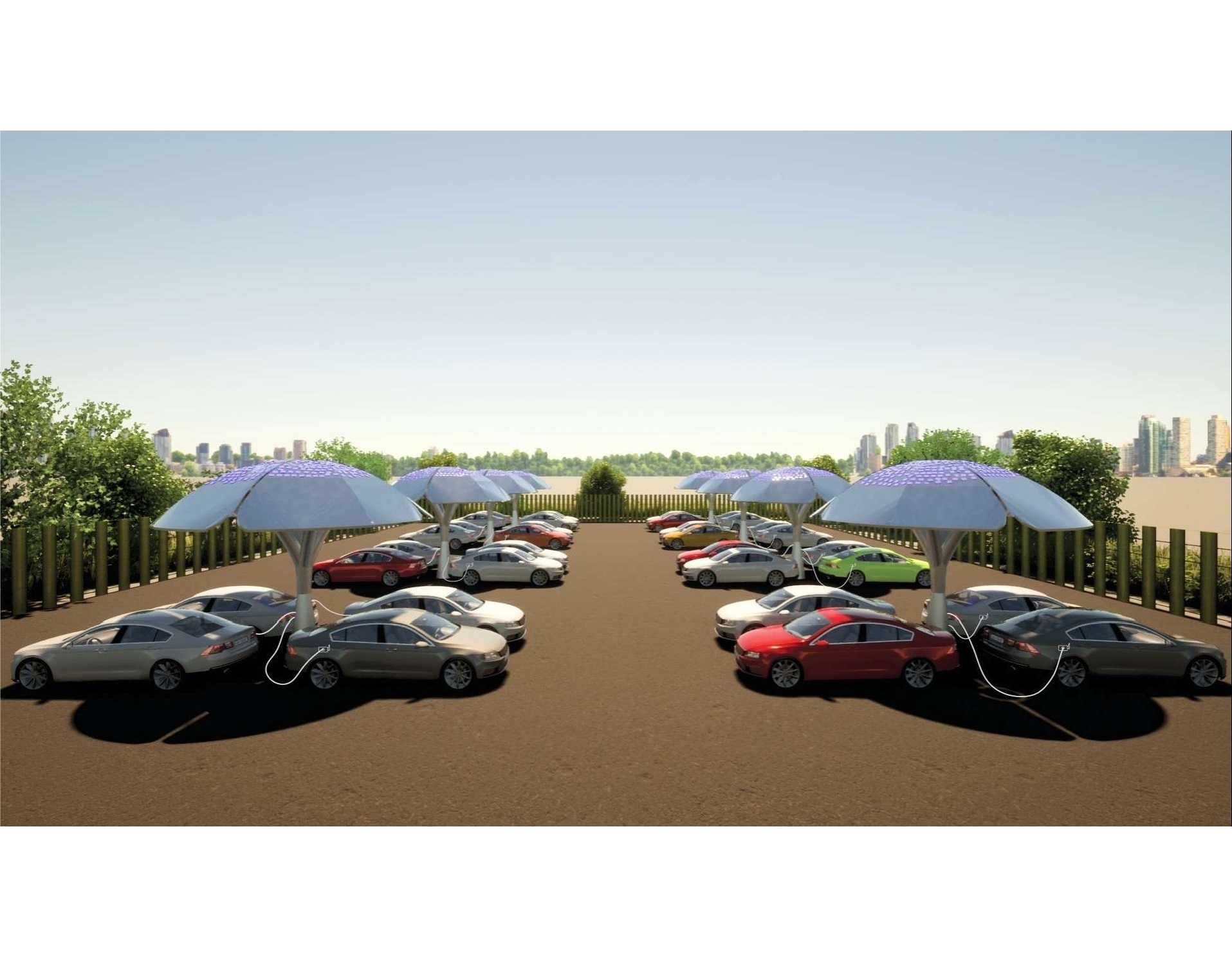
Jülich, 16 April 2021 – There is no cheaper way to generate electricity today than with the sun. Power plants are currently being built in sunny locations that will supply solar electricity for less than two cents per kilowatt hour. Solar cells available on the market based on crystalline silicon make this possible with efficiencies of up to 23 percent. Therefore they hold a global market share of around 95 percent. With even higher efficiencies of more than 26 percent, costs could fall further. An international working group led by photovoltaics researchers from Forschungszentrum Jülich now plan to reach this goal with a nanostructured, transparent material for the front of solar cells and a sophisticated design. The scientists report on their success of many years of research in the renowned scientific journal "Nature Energy".
Silicon solar cells have been steadily improved over the past decades and have already reached a very high level of development. However, the disturbing effect of recombination still occurs after the absorption of sunlight and the photovoltaic generation of electrical charge carriers. In this process, negative and positive charge carriers that have already been generated combine and cancel each other out before they could be used for the flow of solar electricity. Special materials with a special property - passivation - help against this. "Our nanostructured layers offer precisely this desired passivation," says Malte Köhler, former PhD student and first author from the Jülich Institute for Energy and Climate Research (IEK-5), who has since received his doctorate. In addition, the ultra-thin layers are transparent - so the incidence of light is hardly reduced - and exhibit high electrical conductivity.
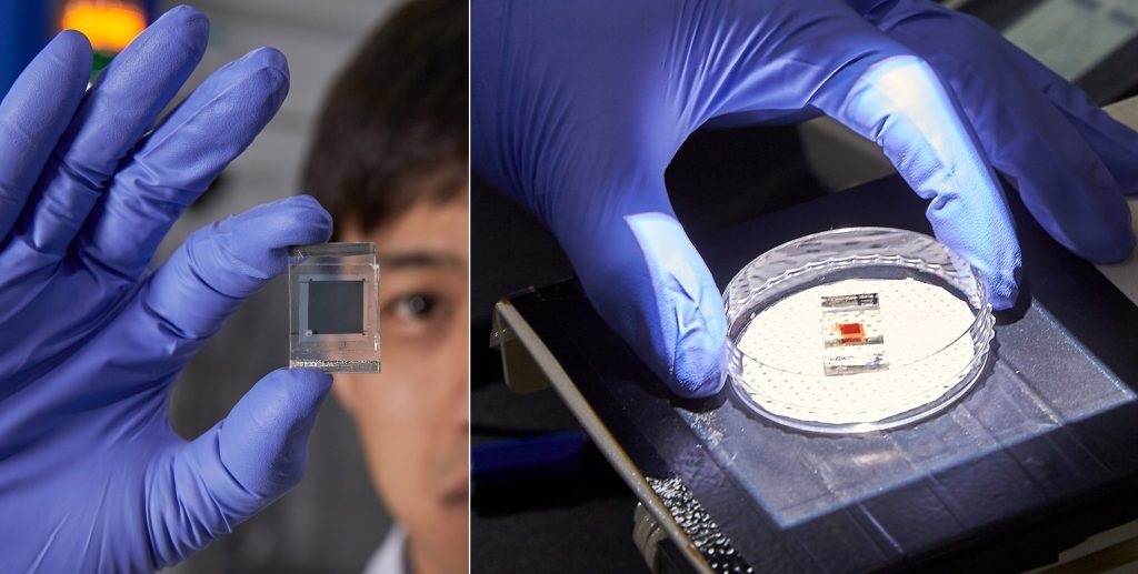
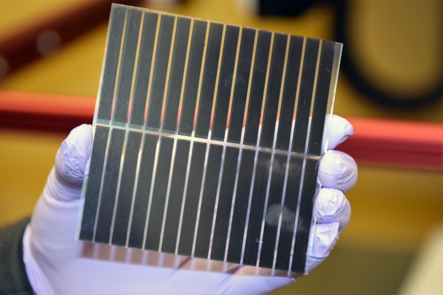
"No other approach so far combines these three properties - passivation, transparency, conductivity - as well as our new design," says Dr. Kaining Ding, head of the Jülich working group. A first prototype of the Jülich TPC solar cell achieved a high efficiency of 23.99 percent (+- 0.29 percent) in the laboratory. This value was also confirmed by the independent CalTeC laboratory of the Institute for Solar Energy Research in Hamelin (ISFH). This means that the Jülich TPC solar cell still ranks slightly below the best crystalline silicon cells made in laboratories to date. But simulations carried out in parallel have shown that efficiencies of more than 26 percent are possible with TPC technology. "In addition, we have only used processes in manufacturing that can be integrated relatively quickly into series production," Ding emphasizes the advantage over other research approaches. With this strategy, the Jülich scientists pave the way for their development from the laboratory to a large scale in industrial solar cell production without too much effort.
Several process steps were necessary to produce the layers of the TPC solar cell.. On a thin layer of silicon dioxide, the researchers deposited a double layer of tiny pyramid-shaped nanocrystals of silicon carbide - applied at two different temperatures. Finally, a transparent layer of indium tin oxide followed. Ding and colleagues used wet chemical processes, chemical vapor deposition (CVD) and a sputtering process.
For their success, the Jülich researchers from IEK 5 and the of the Jülich Ernst Ruska Center for Electron Microscopy worked closely with several institutes in the Netherlands, China, Russia and Ecuador. The partners include researchers from RWTH Aachen University, the University of Duisburg-Essen, the Technical Universities of Delft and Eindhoven, the Universidad San Francisco de Quito, the University and Kutateladze Institute of Thermophysics in Novosibirsk and Sun Yat-Sen University in Guangzhou. In further steps, Kaining Ding's research group plans to further optimize the power yield of its TPC solar cells. "We expect solar cell manufacturers to show great interest in our technology," Ding says.
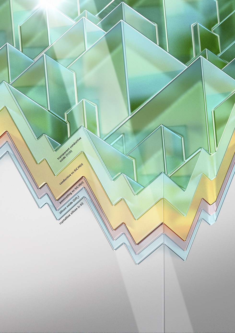
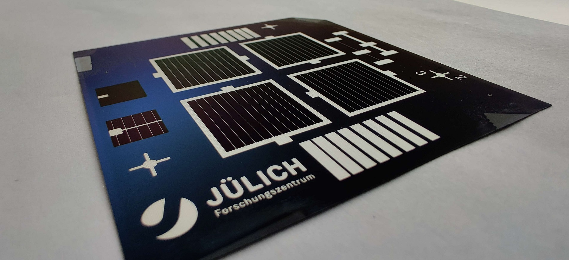
Layer sequence of the new solar cells with transparent frontal layers (TPC, Transparent Passivating Contact) on a wafer with random pyramid structure. The gray area corresponds to the n-doped crystalline silicon wafer, the light blue layer is the wet-chemically grown silicon dioxide, the red layer corresponds to the passivating silicon carbide, followed by the conducting silicon carbide in orange. The green, final layer corresponds to the indium tin oxide (ITO).
Copyright: Forschungszentrum Jülich
Original publication:
Malte Köhler et al.
A silicon carbide-based highly transparent passivating contact for crystalline silicon solar cells approaching efficiencies of 24%
Nature Energy, 15. April 2021, DOI: 10.1038/s41560-021-00806-9