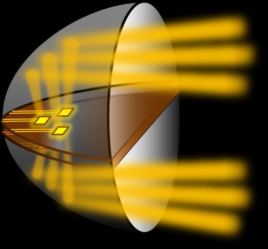
June 2, 2015 – Leuven (Belgium) – FUJIFILM Corporation (President: Shigehiro Nakajima) (hereafter, “Fujifilm”) and nano-electronics research institute, imec (CEO: Luc Van den hove), have demonstrated full-color organic light-emitting diodes (OLED)*1 by using their jointly-developed photoresist technology*2 for organic semiconductors, a technology that enables submicron*3 patterning. This breakthrough result paves the way to producing high-resolution and large organic Electroluminescent (EL) displays and establishing cost-competitive manufacturing methods.
Organic EL displays are increasingly used for televisions, mobile devices including smartphones as well as wearable devices. Since they can be made thin and flexible, while also offering excellent response time and contrast ratio. It is said that today’s products require organic EL displays of high pixel density, i.e. around 200ppi*4 for 4K televisions, 500ppi for full HD mobile devices and even higher density for compact displays for wearable devices. There has been active R&D for organic semiconductors to develop a high-resolution patterning method for organic EL materials to be used in these products.
In 2013, Fujifilm and imec jointly developed photoresist technology for organic semiconductors that enables submicron patterning without damaging the organic semiconductor materials, based on photolithography*5 capable of high-resolution patterning on large substrates. There is no need for additional capital investment since an existing i-line exposure system can be used for the new technology. This is why the technology has attracted wide attention since the development announcement with anticipation of a cost-effective way of manufacturing high-resolution organic semiconductor devices.
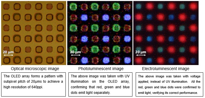
In the latest achievement, Fujifilm and imec produced full-color OLEDs with the photoresist technology for organic semiconductors and successfully verified their performance. Red, green and blue organic EL materials were patterned, each in the subpixel pitch of 20μm*6, to create full-color OLEDs. An OLED array of 40 x 40 dots at the resolution of 640ppi was realized and illuminated with UV rays to confirm that red, green and blue dots separately emitted light. The emission of red, green and blue lights was also confirmed in a test involving the application of voltage rather than illumination, confirming its correct performance.
These results open new opportunities, such as using the novel photolithography in a multiple patterning process. An example would be creating an OLED array that adds a fourth color to red, green and blue, as well as developing previously-unseen devices such as a new sensors that integrate OLED with the organic photodetector*7.
This research result is to be presented at the SID Display Week, one of the world’s largest international exhibitions for information displays, held in San Jose, California from May 31 to June 5, 2015.
Since the commencement of joint research in November 2012, Fujifilm and imec have broken through the boundary of conventional technology to contribute to the progress of technology associated with organic semiconductors, e.g., developing the photoresist technology for organic semiconductors that enables the realization of high-resolution submicron patterns. The two companies will continue to undertake cutting-edge R&D involving semiconductor materials, process technology and system integration, thereby contributing to resolving challenges faced by the organic electronics industry.
About FUJIFILM Corporation
FUJIFILM Corporation, Tokyo, Japan is one of the major operating companies of FUJIFILM Holdings. The company brings continuous innovation and leading-edge products to a broad spectrum of industries, including: healthcare, graphic systems, highly functional materials, optical devices, digital imaging and document products. These are based on a vast portfolio of chemical, mechanical, optical, electronic and thin film coating technologies. In the year ended March 31, 2014, the company had global revenues of $20.8 billion, at an exchange rate of 120 yen to the dollar. Fujifilm is committed to environmental stewardship and good corporate citizenship. For more information, please visit: www.fujifilmholdings.com.
About imec
Imec performs world-leading research in nanoelectronics. Imec leverages its scientific knowledge with the innovative power of its global partnerships in ICT, healthcare and energy. Imec delivers industry-relevant technology solutions. In a unique high-tech environment, its international top talent is committed to providing the building blocks for a better life in a sustainable society. Imec is headquartered in Leuven, Belgium, and has offices in Belgium, the Netherlands, Taiwan, USA, China, India and Japan. Its staff of about 2,200 people includes almost 700 industrial residents and guest researchers. In 2014, imec's revenue (P&L) totaled 363 million euro. Further information on imec can be found at www.imec.be. Stay up to date about what’s happening at imec with the monthly imec magazine, available for tablets and smartphones (as an app for iOS and Android), or via the website www.imec.be/imecmagazine
*1 OLED: Stands for Organic Light-Emitting Diode. Light-emitting elements using organic semiconductors, used for organic EL displays’ pixels
*2 Organic semiconductor: Small molecule organic compounds and polymers carrying the property of a semiconductor
Photoresist: Photosensitive materials that cause photochemical reaction due to light exposures, have different developer solubility at exposed parts and unexposed parts, and are used for microfabrication in semiconductor production.
*3 Submicron: 1/10000mm. 1/10 micron.
*4 ppi: Stands for pixels per inch. This is a unit of pixel density for information displays. It refers to the number of pixels in one inch.
*5 Photolithography method: A film is formed by coating photoresist onto the substrate to be processed, and photochemical reaction occurs within the resist film by exposing patterns through the mask. This microfabrication method forms a mask-like resist pattern on the substrate through development, and transfers the resist pattern onto the substrate as protective material for etching.
*6 Subpixel pitch: Subpixel refers to pixel (red, green, blue, etc.) of the smallest unit. Subpixel pitch represents the midpoint distance between two neighboring subpixels.
*7 Organic photo detector: Photodetection element using organic semiconductors