Moirans/Grenoble (France) – 10th of April, 2013 – NikkoIA SAS carries on its organic image sensors technology developments by extending its sensitivity to X-rays, and validates its compatibility with substrates based on CMOS technology.
NikkoIA announces the production of several innovative organic image sensors, thereby confirming the potential of its technology, and validates the technology building blocks that can be immediately implemented to build its product lines.
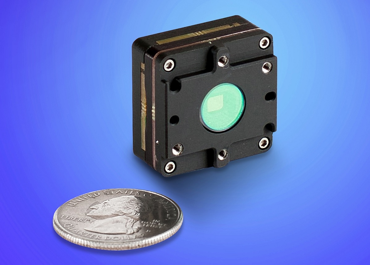
NikkoIA’s technology consists in depositing thin films of photosensitive organic materials onto active or passive reading substrates. Current products are mainly based on TFT backplanes on glass, with a sensitivity optimized in the visible and/or 700/900nm spectrum range. The first evaluation cameras based on these sensors have already been shipped to the company customers.
NikkoIA announces the application of its organic imaging technology to two new product families:
1.X-ray sensitive image sensors, based on 256×256, 98µm-pixels organic image sensors, coupled with a CsI scintillator optimized for 70-90keV energy ;
2.VGA CMOS sensors with 15µm-pixels based on organic photodiodes and CMOS pixel arrays.
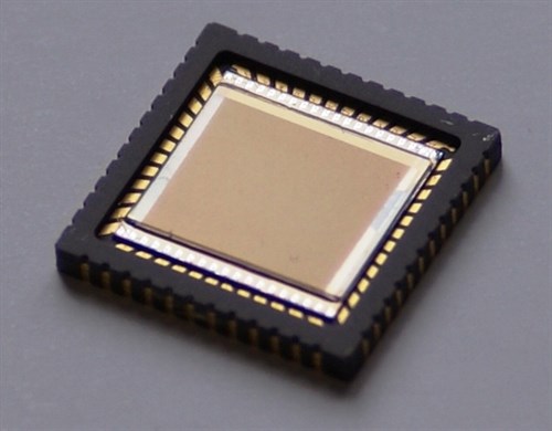
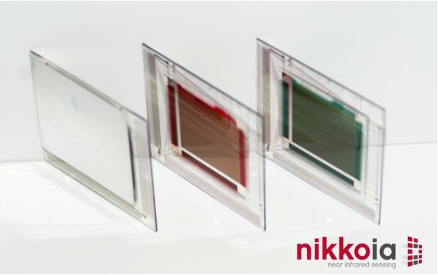
CMOS VGA organic image sensor
The extension of the sensitivity to the X-rays range and the application of NikkoIA’s technology to various types of substrates (TFT or CMOS) enables, in the very short term, the production of large area visible, IR or X-rays image sensors at an extremely competitive cost structure compared to existing technologies, as well as the production of CMOS image sensors sensitive in the infrared beyond the cut-off wavelength of the silicon” said Alain Jutant, President of NikkoIA SAS.
These developments especially enable the production of image sensors immediately interesting for dental radiography and some security applications. They also enable other combinations such as the production of small size, high resolution, SWIR-sensitive CMOS image sensors at a very low cost structure, opening up new imaging solutions in the medical or automotive markets.
These milestones reinforce our technology potential and validate our development strategy. They represent significant achievements that can now be implemented in products dedicated to our target markets », Alain Jutant added.
NikkoIA has a unique position in the market thanks to its worldwide and exclusive license agreement with Siemens AG, granting access to a strong intellectual property protected by several key patents. The company carries on its developments by the sensitivity extension beyond 1300nm while developing at the same time the first products dedicated to its target markets.
NikkoIA SAS
NikkoIA SAS is an industrial company designing, manufacturing and selling selective or broadband visible and near-infrared image sensors.
NikkoIA’s technology relies on photosensitive materials made of a combination of organic and inorganic components, which are deposited with thin-film manufacturing processes onto standard reading substrates.
NikkoIA’s technology demonstrates similar performances as current InGaAs sensors for a lower cost, and enables the design of very large dimension sensors with pixels from very few to several hundred microns. It enables newapplications in the medical, security and interactive user interfaces areas. NikkoIA SAS can be found on the world wide web at www.nikkoia.com