2022.01.18
- By designing an optical structure with only one material, a semiconductor device capable of absorbing more than 99% of narrowband light and detecting near-infrared light is realized
- Expected to greatly contribute to mass production and commercialization of high-performance optical devices
A structural design technology has been developed that overcomes structural complexity and performance limitations by breaking away from the complicated manufacturing process of existing semiconductor devices, which realizes a high absorption rate with only one material.
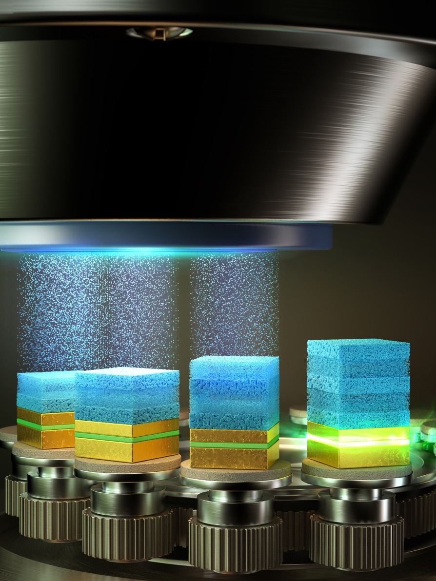
GIST (Gwangju Institute of Science and Technology, President Kiseon Kim) School of Electrical Engineering and Computer Science Professor Young Min Song's research team used a film-type laminated structure (Tamm plasmon structure*), which is a very simple form made of a single material, to selectively absorb in the nearinfrared region and developed a next-generation semiconductor device with high absorption in a narrow band.
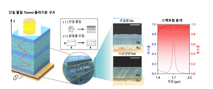
Tamm plasmon structure of a single material capable of high absorption in the near-infrared region
Conventional semiconductor devices have been developed with optical structures in complex shapes of tens to hundreds of nanometers for high absorption and excellent narrowband performance.
However, these structures have limitations in that expensive and complicated manufacturing processes are required, and it is difficult to construct large-area devices, making it difficult to use in actual commercial products.
Recently, to overcome this fabrication method and complexity, a simple film-type semiconductor device, Tamm plasmon structure, has been developed, but it is difficult to achieve 100% absorption due to the use of most common materials, which acts as a limitation for optical design.
To achieve 100% absorption of the light to be detected, the impedance* value must be adjusted so that strong absorption can occur between the DBR** structure and the metal structure. However, due to the limitation of the material constituting the DBR layer, the optical properties are not freely controlled, and this has been a major obstacle in achieving high absorption.
The single-material-based Tamm plasmon structure developed by the research team imparts porosity to the material and freely modulates the properties of the material. As a result, it showed an absorption rate of more than 99%, which is close to perfect absorption.
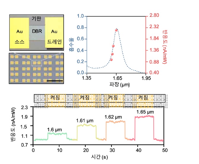
Implementation of next-generation semiconductor devices with selective reactivity in the form of an array
This technology showed strong absorption and narrowband high-speed light detection characteristics (47~76ms) even with a simple structure. In addition, it succeeded in realizing a large-area process at the wafer level, confirming the applicability to commercial products.
GIST Professor Young Min Song said, "We developed a structural design method that overcomes the structural complexity and performance limitations of existing semiconductor devices and realizes a high absorption rate with only one material by controlling material properties. By grafting this technology, it is expected that this can be applied to various optical devices such as solar cells based on light absorption/emission and passive radiation structures."
This research was supported by the future material discovery project of the Ministry of Science and ICT, the Korea Research Foundation, Nano and Material Technology Development Project, the Institute of Information & Communications Technology Planning & Evaluation, and the GIST Research Institute and was published online on January 10 in the international scientific journal Advanced Optical Materials (IF: 9.926).
* Tamm plasmon structure: A structure in which a layer in which different dielectric layers are periodically stacked and a metal layer are combined, and strong absorption of light occurs at the interface between the two layers. In this study, the improved optical properties in the near-infrared region were utilized through the Tamm plasmon structure.
* impedance: The wave impedance of electromagnetic waves represents the ratio of electric and magnetic fields.
** Distributed Brgg Reflectors (DBR): It is a multilayer structure in which materials with different refractive indices are periodically stacked.


