July 1, 2020
Hamamatsu Photonics succeeded in developing a liquid-crystal spatial light modulator (SLM) having the world’s highest pulse laser power capability up to 400 GW/cm2, by utilizing our advanced thin-film and circuit designing technologies. This new SLM to high-power industrial pulsed laser systems will contribute to achieve high-throughput, high-precision laser processing to processing resistant material such as light-weight and high-strength carbon fiber reinforced plastics (CFRP).
This work is partially supported by Council for Science, Technology and Innovation (CSTI), Cross-ministerial Strategic Innovation Promotion Program (SIP), "Photonics and Quantum Technology for Society5.0"(Funding agency: National Institutes for Quantum and Radiological Science and Technology, QST).
Aim of this project is to prove and demonstrate innovative manufacturing and fabrication techniques by using a cyber-physical system (CPS) that combines cyberspace (virtual space) and physical space (real space) to a highly advanced degree. SLM can freely control the irradiation pattern of laser, this device is viewed as an essential for new manufacturing and fabrication techniques that utilize artificial intelligence (AI) such as CPS-type laser processing systems.
Development background
The “Photonics and Quantum Technology for Society 5.0” is SIP second term project and includes three areas as R&D themes or namely laser processing, photonic quantum communication and photonics & electronic information processing which are technological elements constituting CPS and deemed to need further technological innovation. Among these we have already started R&D work on laser processing of processing resistant materials while aiming to demonstrate innovative manufacturing techniques by using a CPS-type laser processing system. In the CPS-type laser processing system, processing sample is irradiated with laser under many different conditions and the data from the processing results are collected and analyzed by using AI to find optimal processing conditions. This will shorten the time required for manual trial-and-error procedures and achieve laser processing with an optimized design and production process. As a company participating in R&D for “Photonics and Quantum Technology for Society 5.0,” we have made an effort to improve SLM performance.
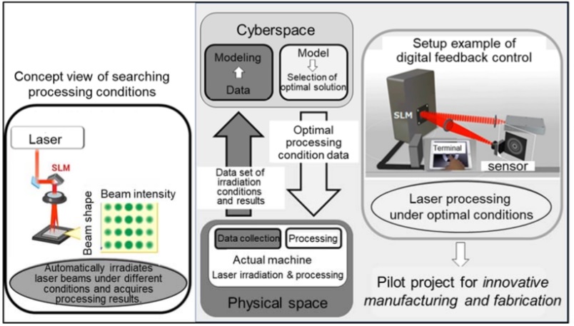
Applying newly developed SLM to CPS-type laser processing systems
How the SLM operates
A spatial light modulator or SLM is an optical device utilizing liquid crystals to control the wavefront( *) of incident light such as lasers to freely modulate the wavefront shape of the reflected light. A liquid crystal layer is sandwiched between a silicon substrate with pixel electrodes and a glass substrate with transparent electrodes. The path length of the incident light is varied by controlling the inclination of each liquid crystal according to the signal sent to the pixel electrodes from a PC, and the reflected light is in this way modulated to allow freely controlling the laser irradiation pattern for example to branch the incident light or correct its distortion.
* Wavefront of light: Light has both wave and particle properties. The wavefront of light is a plane formed by connecting points with waves at the same height at a particular timing when light propagates as a wave. Light travels perpendicular to the wavefront
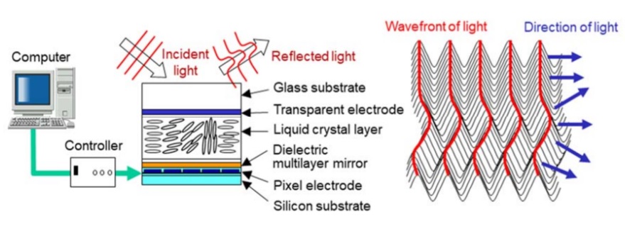
How the SLM works (left) and direction of light (right)
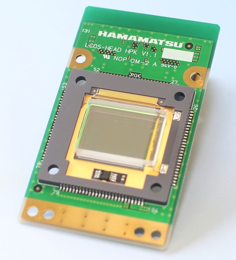
Product overview
This product is an SLM having the world’s highest pulse laser power capability and developed for use with high-power industrial pulsed lasers.
Lasers are broadly classified into CW (continuous wave) lasers that emit a continuous light beam at a constant power, and pulsed lasers that repeatedly emit light pulses at short time intervals. Currently, CW lasers are the mainstream of laser machining since they can be used for heat treatment of metallic materials such as laser welding and cutting. Pulsed lasers, on the other hand, can emit light pulses with momentarily high energy allowing high-precision laser machining with minimal heat damage. Because this precision is higher than conventional mechanical machining, pulsed laser machining is becoming widely used for processing resistant materials such as CFRP and low dielectric constant (low-k) materials that prevent a drop in operating speed in semiconductor integrated circuits. However, several issues are remained such as the machining speed and processing throughput. Incorporating an SLM into an industrial pulsed laser system allows irradiating diffracted multiple laser beams onto different points of target sample simultaneously. This improves the processing throughput compared to laser machining that uses only a single focused beam, but so far the output power required for machining has been inadequate. Due to this situation, industrial pulsed lasers with higher output power are becoming available on the market which also creates an increasing demand for SLM having even higher resistance to laser power.
Hamamatsu Photonics has already developed and produced optical wavefront control devices with high resistance to light mainly for laser marking applications for engraving characters and QR codes on objects moving at high speed on production lines. This time, by reviewing the thin-film design for dielectric multilayer mirrors that reflect the incident laser and by redesigning the pixel electrode circuit, Hamamatsu Photonics succeeded in increasing the light resistance up to 400 GW/cm2 which is more than 10 times higher than Hamamatsu Photonics previous products.
Conventional dielectric multilayer mirrors consist of multiple layers made of two types of alternately evaporated material films. At the boundary where these thin films are in contact, the light often interferes with or reinforces other light, posing the problem that the thin films may be damaged when a high power laser beam is incident on them. To solve this problem, we optimized the thin-film design via numerical simulation to suppress the interference of light at the boundaries and succeeded in minimizing adverse effects on the thin films. We also suppressed unwanted noise by redesigning the pixel electrode circuit.
Using this newly developed SLM with a higher power pulsed laser allows simultaneously irradiating a target sample with multi-beams while maintaining adequate output power and in this way helps achieve high-throughput, high-precision laser processing of processing resistant materials such as CFRP used for aircraft and transportation equipment and low-k materials used for 5th generation mobile communication system (5G).
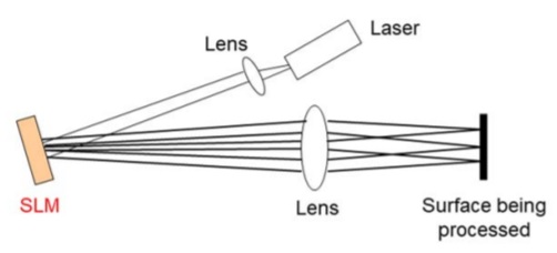
Pulse laser processing using an SLM
Future approaches
Hamamatsu Photonics is making further progress in improving these light resistance properties. This year we will complete a highly light-resistant SLM to install in the CPS-type laser processing system of the University of Tokyo and also in the actual working platform of the laser processing machine at the Utsunomiya University Center for Optical Research & Education. We believe this will contribute to industry and society.