March 30, 2020
Thanks to the expertise in integrated photonics of the Centre de Nanosciences et de Nanotechnologies - C2N and in quantum photonics of the Institut de Physique de Nice – INPHYNI, a team of physicists have developed a new silicon photonic chip architecture. This type of photonic chip is genuinely compliant with telecommunication standards.
Quantum information technologies are identified as major emerging key technologies, with protocols allowing absolute security in data exchange and massively parallel processing capabilities. These quantum advantages are based on the exploitation of properties that are exclusive to quantum physics, such as entanglement. For enabling quantum communication across metropolitan networks, actual quantum systems have to be developed along reliable, functional, and scalable architectures. Photonics integrated on silicon stands as one of the key solutions to meet these requirements. It permits the dense integration of linear and non-linear optical functionalities on monolithic substrates, encompassing generation, routing, advanced manipulation, as well as detection of photonic quantum states. Such a level of integration remains a major challenge, mainly due to the limited performance of on-chip optical pump rejection filters. The latter must reduce the laser pump by more than 9 orders of magnitude while preserving photon-pair entanglement.
Researchers from the Centre de Nanosciences et de Nanotechnologies - C2N (CNRS/Université Paris-Saclay) and from the Institut de Physique de Nice – INPHYNI (CNRS/Université Côte d’Azur) have joined their expertise to develop a novel, telecom compliant, silicon chip integrating both a non-linear photon-pair generator and a passive pump rejection filter. The researchers have thus qualified the entanglement out of such an innovative photonic circuit and demonstrated its applicability to quantum communication networks. This work has recently been published in the journal npj Quantum Information.
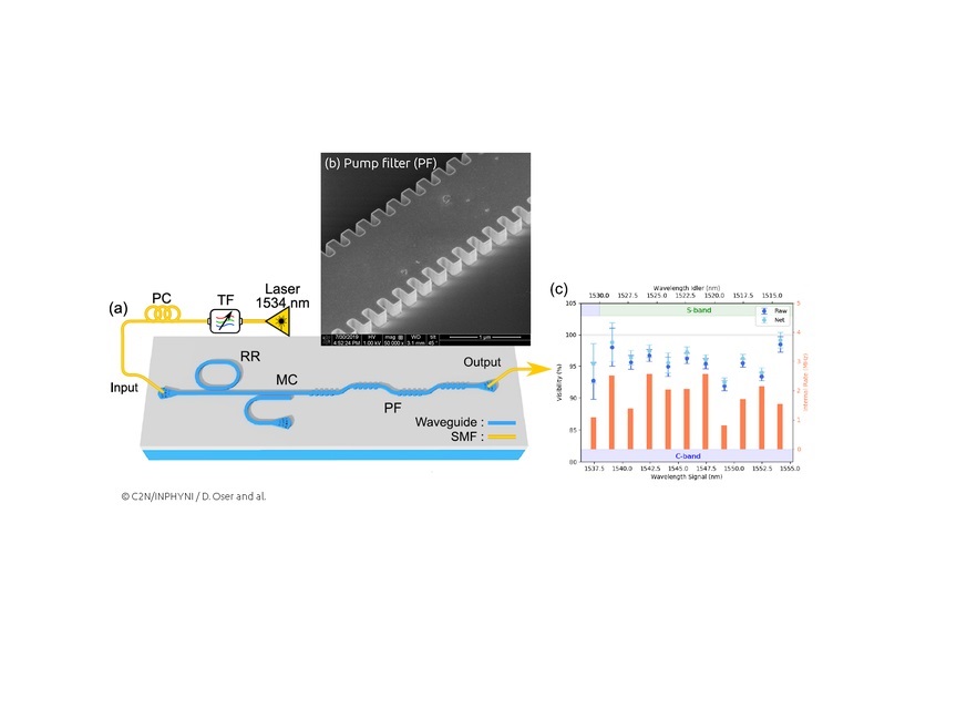
The experimental setup (see figure) consists in a continuous-wave laser pumping a photonic chip fabricated at the C2N, in which a micro-cavity generates, through four-wave mixing, pairs of entangled photons. Preserving the quantum properties of information requires high filtering of the pump laser. The breakthrough of this demonstration lies in the design and realization of a filtering stage integrated directly on the chip for attenuating, at a tremendous level, the guided pump signal compared to the quantum signal. The proposed approach exploits a multimode waveguide with an all-passive Bragg corrugation (a periodic variation of the waveguide width that reduces the impact of fabrication errors). This generic strategy leads to high rejection rates without requiring the use of active control and the realized filter shows a record rejection estimated at more than 85 dB over a 5 nm bandwidth with losses equivalent to that of a standard silicon waveguide.
Energy-time entangled photons are naturally produced over a frequency-comb matching the channel-grid of the telecom C-band, symmetrically to the pump channel. Researchers at the INPHYNI have demonstrated the first entanglement qualification, showing the highest raw quantum interference visibility (exceeding 92 % ) obtained to date with such a stand-alone circuit. This demonstration therefore attests the validity of the approach for the filtering stage.
These results will certainly further promote the development of more advanced and scalable photonic-based quantum circuits, compliant with telecommunication standards. In the perspective of a large-scale deployment over telecommunication networks, a partnership has been established with a global semiconductor company able to produce such integrated circuits with world-class manufacturing capabilities.
References:
High quality photonic entanglement out of a stand-alone silicon chip
Dorian Oser1, Sébastien Tanzilli2, Florent Mazeas2, Carlos Alonso Ramos1, Xavier Le Roux1, Grégory Sauder2, Xin Hua2, Olivier Alibart2, Laurent Vivien1, Éric Cassan1, and Laurent Labonté2
npj Quantum Information (2020)
DOI : https://doi.org/10.1038/s41534-020-0263-7
1 Centre de Nanosciences et de Nanotechnologies – C2N (CNRS, Université Paris-Saclay), Palaiseau
2 Institut de Physique de Nice – INPHYNI (CNRS/Université Côte d’Azur)


