May 06, 2020
The research group of Professor Erez Hasman, head of Technion’s nano-optics laboratory, recently published a pioneering paper in the Nature Nanotechnology. The research was led by Dr. Bo Wang in collaboration with Dr. Kexiu Rong, Dr. Elhanan Maguid, and Dr. Vladimir Kleiner.
Electronic chip technology, nano-mechanics, and nano-photonics deal with components on the nanometric scale, requiring extremely precise quality control of the chip production process. An inaccuracy of more than a few nanometers will cause the chip to malfunction. In the micro-nanoelectronics field, chip quality is tested using an electron-beam microscope, where the chip is placed in a deep vacuum chamber. This is an extremely long and complicated process that precludes extensive production control. Quality control using optics overcomes this problem since the measurement is carried out without vacuum and is rapid; however, because of the light’s wavelength, it is not sufficiently precise.
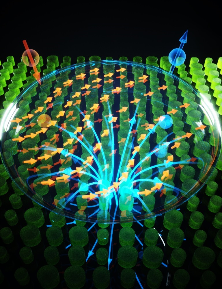
The solution devised by Prof. Hasman’s research group is based on intensive scientific research in fields that combine the interaction of light and materials with magnetic fields. Electronic chips consist of nanometric components that must be very precise and uniform (they cannot differ by more than 1-5 nanometers) in a cycle that is smaller than a wavelength of visible light. Therefore, if the chip is illuminated, the light reflected or transmitted from it will make it impossible to measure the nanometric dispersal ― a critical parameter for the chip’s functioning.
This scientific breakthrough combines operating a magnetic field in an optical microscope and illuminating with polarized light on ferromagnetic meta-atoms displaying nanoscale disorders. This splits the light beam angle as such that the light is reflected as two beams with opposite circular polarizations (in scientific language, circular polarization is called ‘photonic spin’―photon being a light particle). The split angle is tiny and therefore the researchers use a technique known as “weak measurement” that Prof. Yakir Aharonov of Tel Aviv University suggested for quantum measurements.
In addition to the already discussed, this discovery opens the doors to new possibilities for measuring extremely small disorders in magnetic fields and in magnetism of various materials, as well as researching various fluctuation phenomena in quantum mechanics and other areas.
According to Prof. Hasman, “Publishing the research in this prestigious journal shows that even during difficult times, such as the current coronavirus crisis, Technion continues to publish groundbreaking articles in leading scientific journals. Our research group includes scientists from a variety of disciplines, including physics, materials, and engineering, studying fundamental science and applied research that lead to numerous applications in the high-tech industry. This interdisciplinary research leads to growing numbers of successes that have an impact on scientific advancement and on the development of important and diverse technological applications.”
The research was supported by the Israel Science Foundation, the Israel Ministry of Science, Technology and Space, the United States−Israel Binational Science Foundation (BSF), the U.S. Air Force Office of Scientific Research and, in part, by Technion via an Aly Kaufman Fellowship. The fabrication was performed at the Micro-Nano Fabrication & Printing Unit (MNF&PU), Technion. The lab’s website is hasman.technion.ac.il
Click here for the paper in Nature Nanotechnology


