July 8, 2019
Denis Paiste | Materials Research Laboratory
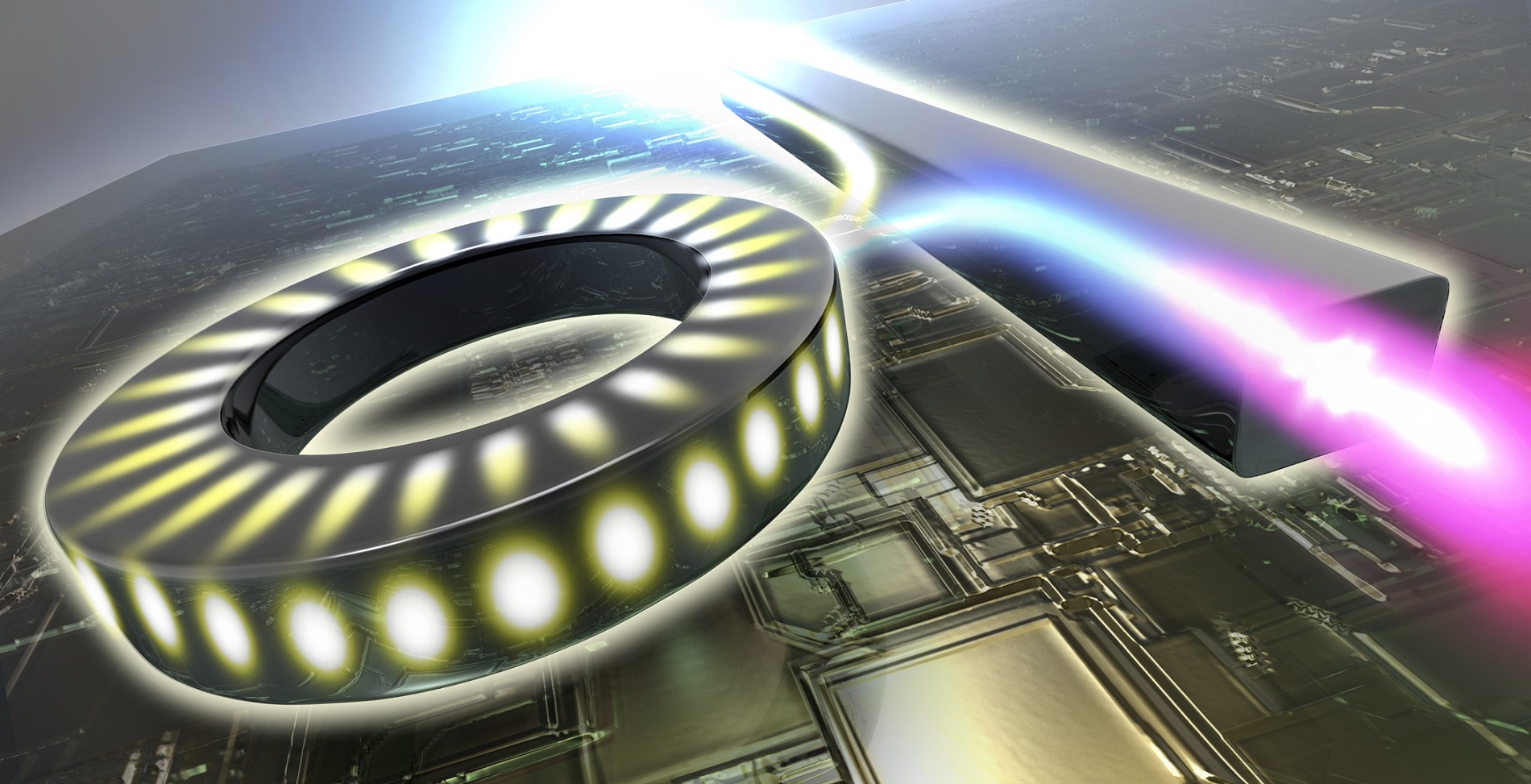
Researchers at MIT and Singapore University of Technology (SUTD) have demonstrated a micro ring resonator made of amorphous silicon carbide with the highest quality factor to date. The resonator shows promise to be used as an on-chip photonic light source at the infrared telecom wavelength of 1,550 nanometers.
Ordinary daylight will pass through a window unaltered, in a process called linear transmission, but the same light passing through a prism will split into a rainbow of colors. Similarly in photonic devices, infrared light from a laser can pass through in linear fashion without changing its “color,” but at high intensity, the light can exhibit nonlinear behavior, generating additional colors, or wavelengths. For example, a single yellow laser coupled to a photonic device can generate blue, green, yellow, or orange colors.
Researchers led by MIT Materials Research Laboratory Research Scientist Anuradha M. Agarwal fabricated the amorphous silicon carbide ring resonators, and researchers at SUTD led by Associate Professor Dawn T.H. Tan analyzed the device’s linear and nonlinear properties.
“We are able to show one order of magnitude higher nonlinear effect than measured before in any of the silicon carbide substrates,” Agarwal says.
Quality factor is a measure of how strongly the resonator produces nonlinear effects. “The larger the quality factor, the better the nonlinear effect,” says Tan, who leads the Photonics Devices and Systems Group at SUTD. “So in this case, the quality factor was pretty good. It was actually much better than we expected.”
The findings are described in a paper, featured on the cover of ACS Photonics, by Agarwal, Tan, MIT materials science and engineering graduate student Danhao Ma, and three others in Singapore and Malaysia.
Resonator advantage
High intensity of light is needed to trigger nonlinear properties for photonic devices, which can be achieved either by ramping up the power of the laser or using a device such as a ring resonator. “A ring allows for that high intensity because it traps the photons for a long time,” Agarwal explains. “More and more photons build up to like a crescendo and that allows for the evaluation of nonlinear optical properties.”
Like a fiber optic cable, which transmits light by wrapping one material that carries the light inside a different material that won’t allow the light to pass through it, the amorphous silicon carbide ring resonator and straight waveguide for carrying the infrared light are surrounded by a layer of silicon oxide that minimizes the amount of light that can escape. The refractive indices of different materials determine how well they work together as the carrier layer and protective outer layer.
“We are trying to create this kind of a fiber optic waveguide on chip,” Agarwal explains. “So it’s like a fiber, but on a chip, and therefore what we need is a core with a high (refractive) index and a cladding with a low index.” Silicon carbide and silicon oxide have a large enough difference in their refractive indices that they work together well as the core and cladding for a waveguide.
The researchers achieved the record quality factor in this study using the plasma enhanced chemical (PECVD) process to deposit the silicon carbide, at a temperature that is compatible with complementary metal-oxide semiconductor (CMOS) silicon chip processing, and developing a method to pattern and etch the silicon carbide ring resonator, which is coupled to a straight waveguide.
Overcoming challenges
MIT graduate student Ma overcame several processing challenges to make the high-quality resonator. When Ma began working on silicon carbide materials for this study about three years ago, there was no existing recipe for how to etch a pattern into the amorphous silicon carbide material when it is deposited on a silicon dioxide substrate. “Silicon carbide is a very rigid and physically and chemically hard material, so, in other words, it’s very difficult for it to be removed or etched,” Ma says.
To deposit and etch the silicon carbide waveguide on silicon oxide, Ma first used electron beam lithography to pattern the waveguides and reactive ion dry etching to remove excess silicon carbide. But his first attempts using a typical polymer-based mask didn’t work because the process removed more of the mask than the silicon carbide. Ma then tried a metal mask, but grain boundaries from the mask carried over to the silicon carbide, leaving behind rough sidewalls in the waveguides. Roughness is undesirable because it increases photon scattering and light loss. To resolve the issue, Ma developed a technique using a silicon dioxide-based mask for the reactive ion etching. During the process development, Ma worked closely with Qingyang Du, an MIT postdoc, and Mark K. Mondol, assistant director of the NanoStructures Laboratory in the MIT Research Laboratory of Electronics.
“We came up with the right type of chemistries in this reaction and controlled the gas flows and the plasma, or, in other words, the details of the processing recipe,” Ma says. “This recipe is really selective to etch silicon carbide compared to silicon dioxide, which made it possible for us to shape the silicon carbide photonic devices and have a smooth waveguide sidewall,” Ma says. The smooth sidewall is critical for maintaining the optical signals in the photonic device, he notes.
The main sources of light loss in these resonators are absorption of photons in the ring material and/or scattering of photons caused by edge roughness of the ring device. “Danhao’s processing yielded smooth sidewalls, which enabled low loss and a high Q (quality) factor resonator,” Agarwal explains.
“The beauty of this silicon carbide material and the technique that we used here in the paper is that the PECVD process of silicon carbide is an inexpensive process, standard in the silicon microelectronics industry,” says Ma, whose research concentration is materials design and engineering for integrated photonics. “Use of the existing microelectronics processes will make the adoption of silicon carbide into the integrated photonic and integrated electronic platforms easier.” The PECVD and reactive dry ion etching processes he used don’t require the lattice matching and other critical demands of epitaxial growth on silicon, and is substrate-agnostic, Ma says.
Better performance
Tan has studied silicon nitride materials and other CMOS materials for their nonlinearity for several years. “For (amorphous) silicon carbide, you would have a better enhancement when cast as a resonator compared to ultra-silicon-rich nitride, and it also has a higher nonlinear refractive index than stoichiometric silicon nitride, which is prolific in nonlinear optics,” Tan says.
Several kinds of photon absorption known as two-photon and three-photon absorption are typically present in these devices. In this study, Tan says, loss was dominated by three-photon absorption, which is a relatively weak nonlinear loss mechanism, while two-photon absorption, which can be a problem in many crystalline silicon and amorphous silicon materials, was suppressed.
Agarwal and Tan began collaborating while Tan was a visiting scholar at MIT from August 2013 through August 2014. “We were very fortunate to be paired with Professor Tan’s team, and we benefited a great deal from this collaboration, and we continue to collaborate,” Agarwal says. Agarwal’s team previously worked on using silicon carbide in a sensor for harsh environments.
For the current work, the Singapore team measured the additional wavelengths of light generated in the ring resonator — a phenomenon called spectral broadening, which is quantified by a term called Kerr nonlinearity. The researchers found the Kerr nonlinearity of their silicon carbide film to be almost 10 times that of previously reported crystalline and amorphous silicon carbide.
“With this you see a spectral broadening effect, which we can leverage to our advantage because now instead of having just one frequency, we are generating several other frequencies which can provide a super continuum light source,” Agarwal says.
Exciting development
Professor David J. Moss, director of the Centre for Micro-Photonics at Swinburne University of Technology in Australia, who studies photonic materials, says, “This paper presents new results for amorphous silicon carbide as a promising CMOS-compatible platform for nonlinear optics, particularly focused on the important telecommunications window.”
“The achievement of a high Kerr nonlinearity — comparable to crystalline silicon — along with negligible two-photon absorption, together with record high (for silicon carbide) Q factor ring resonators, is an exciting development in the continuing quest for ever-more-efficient platforms for nonlinear optics at 1,550 nanometers,” adds Moss, who was not involved in this research.
Associate Professor Andrea Melloni, who heads the Photonics Devices Group at Politecnico di Milano in Italy, says, “Amorphous SiC (silicon carbide) deposited with PECVD is of great interest. The refractive index is extremely appealing (2.45 is not a common value) because it is high enough to allow large-scale integration, but not as high as silicon, thus minimizing problems associated with the very high index contrast of SOI (silicon-on-insulator) structures.” Melloni, who also did not participate in this research, published a paper last year on Silicon Oxycarbide Photonic Waveguides.
Looking ahead, Ma hopes to make a thicker silicon carbide waveguide for a broader set of applications — for example, creating more wavelengths (multiplexing) within the single waveguide.
“As a first demonstration of what we’ve done together, I think it’s a very promising platform where if we can continue refining the platform and device design, I think we probably would be able to demonstrate very good resonator enhancement because we have demonstrated very good quality factors,” Tan says. “If we wanted to do something like a frequency comb or an optical parametric oscillator, the threshold power becomes a lot smaller if the quality factor is large.”
“If this work can be jointly funded then we can think about making an integrated light source, sensor and detector, so there are a lot of exciting next steps in this,” Agarwal says.
This work was supported by SUTD–MIT International Design Center, the Singapore National Research Foundation, and the Singapore Ministry of Education.


