(Tokyo, March 2017) Researchers at the Tokyo Institute of Technology (Tokyo Tech) and Nippon Telegraph and Telephone Corporation (NTT) have developed a “spin-resolved oscilloscope.” This device is a basic measuring instrument for plasmonics and spintronics, which are key technologies for future electronics applications. The coupling of light and electronic charges in plasmonics will pave the way for ultra-high-speed information processing, whereas spintronics will provide low-energy-consumption technology in a highly information-oriented society. The spin-resolved oscilloscope pioneers future “spin-plasmonics,” where ultra-high-speed low-energy-consumption devices will be achieved.
An electron has charge and spin, and both the charge- and spin-density excitations in an electronic system can be utilized in information processing. The dynamics of charge-density waves has been investigated in plasmonics, and that of spin-density waves has been studied in the field of spintronics. However, less effort has been devoted to combining these two technologies and to developing the expected ultra-high-speed and low-energy-consumption devices. To date, a major obstacle preventing the promotion of this research field has been the lack of a measuring instrument that is sensitive to both charge and spin.
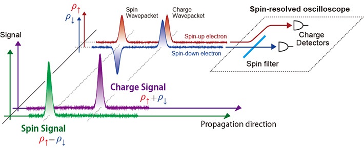
In their recent paper, published in Nature Physics, Dr. Masayuki Hashisaka at Tokyo Tech and colleagues reported a “spin-resolved oscilloscope” that enables measurement of the waveforms of both charge and spin signals in electronic devices. An oscilloscope is a basic measuring instrument used in electronics; however, conventional oscilloscopes do not facilitate both charge and spin measurement.
The “charge signal” is the total charge of the spin-up and -down electron densities. Further, the “spin signal” is the difference between the spin-up and -down electron densities. Both these signals traveling in a semiconductor device can be detected by the spin-resolved oscilloscope, which is composed of a spin filter and nanometer-scale time-resolved charge detectors. The spin filter separates the spin-up and -down electrons, while the time-resolved charge detector measures the waveforms of the charge-density waves. By combining these spintronic and plasmonic devices, the spin-resolved oscilloscope is established.
Using this spin-resolved oscilloscope, Hashisaka and colleagues demonstrated waveform measurements of charge- and spin-density wavepackets in a semiconductor device. They succeeded in observing the spin-charge-separation process in a one-dimensional (1D) electronic system composed of quantum Hall edge channels, which is a prototypical system for the investigation of 1D electron dynamics. This was the first experiment in which a single spin-charge-separation waveform measurement allowed estimation of all the relevant system parameters. Further, this observation manifests not only the usefulness of the spin-resolved oscilloscope, but also the possibility for developing novel plasmonic and spintronic devices based on 1D semiconductor materials.
The spin-resolved oscilloscope will promote investigations in both plasmonics and spintronics; for example, this device will aid studies of electron dynamics in various 1D systems. In addition, the spin-resolved oscilloscope will pave the way for future “spin-plasmonics,” where ultra-high-speed and low-energy-consumption devices will be achieved.
This movie shows the waveform measurements of charge- and spin-density wavepackets in a Tomonaga-Luttinger liquid by the spin-resolved oscilloscope. Continuous reproduction at about 10 times speed.
Authors: M. Hashisaka1*, N. Hiyama1, T. Akiho2, K. Muraki2 and T. Fujisawa1*
Title of original paper: Waveform measurement of charge- and spin-density wavepackets in a chiral Tomonaga-Luttinger liquid
Journal: Nature Physics
DOI: dx.doi.org/10.1038/nphys4062
Affiliations: 1Department of Physics, Tokyo Institute of Technology, 2-12-1-H81 Ookayama, Meguro, Tokyo 152-8551, Japan.
2NTT Basic Research Laboratories, NTT Corporation, 3-1 Morinosato-Wakamiya, Atsugi, Kanagawa 243-0198, Japan.


