New York, NY—April 17, 2017—A team of Columbia Engineering researchers, led by Applied Physics Assistant Professor Nanfang Yu, has invented a method to control light propagating in confined pathways, or waveguides, with high efficiency by using nano-antennas. To demonstrate this technique, they built photonic integrated devices that not only had record-small footprints but were also able to maintain optimal performance over an unprecedented broad wavelength range.
Photonic integrated circuits (ICs) are based on light propagating in optical waveguides, and controlling such light propagation is a central issue in building these chips, which use light instead of electrons to transport data. Yu’s method could lead to faster, more powerful, and more efficient optical chips, which in turn could transform optical communications and optical signal processing. The study is published online in Nature Nanotechnology April 17.
“We have built integrated nanophotonic devices with the smallest footprint and largest operating bandwidth ever,” Yu says. “The degree to which we can now reduce the size of photonic integrated devices with the help of nano-antennas is similar to what happened in the 1950s when large vacuum tubes were replaced by much smaller semiconductor transistors. This work provides a revolutionary solution to a fundamental scientific problem: How to control light propagating in waveguides in the most efficient way?”
The optical power of light waves propagating along waveguides is confined within the core of the waveguide: researchers can only access the guided waves via the small evanescent “tails” that exist near the waveguide surface. These elusive guided waves are particularly hard to manipulate and so photonic integrated devices are often large in size, taking up space and thus limiting the device integration density of a chip. Shrinking photonic integrated devices represents a primary challenge researchers aim to overcome, mirroring the historical progression of electronics that follows Moore’s law, that the number of transistors in electronic ICs doubles approximately every two years.
Yu’s team found that the most efficient way to control light in waveguides is to “decorate” the waveguides with optical nano-antennas: these miniature antennas pull light from inside the waveguide core, modify the light’s properties, and release light back into the waveguides. The accumulative effect of a densely packed array of nano-antennas is so strong that they could achieve functions such as waveguide mode conversion within a propagation distance no more than twice the wavelength.
“This is a breakthrough considering that conventional approaches to realize waveguide mode conversion require devices with a length that is tens of hundreds of times the wavelength,” Yu says. “We’ve been able to reduce the size of the device by a factor of 10 to 100.”
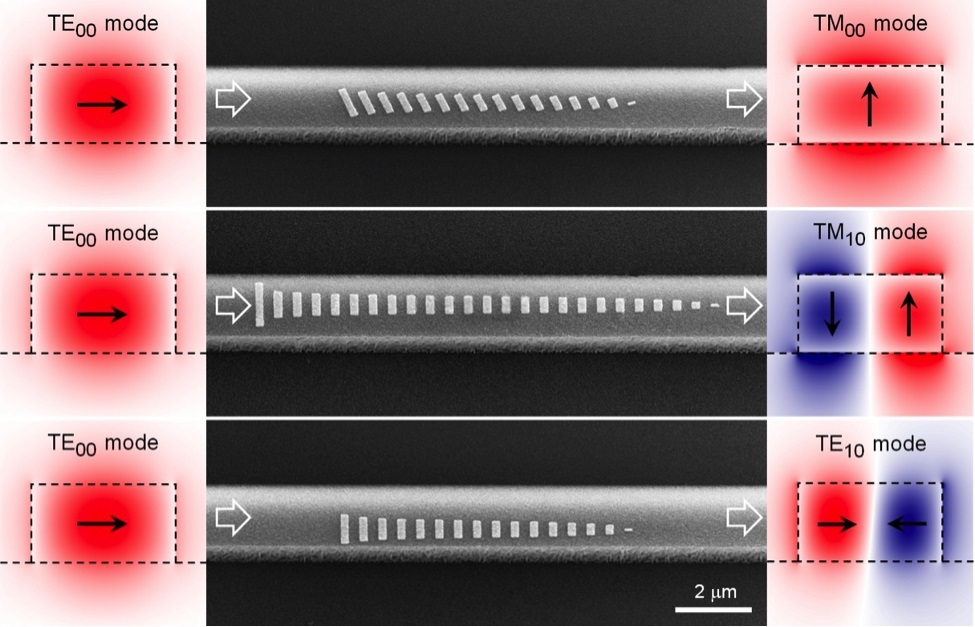
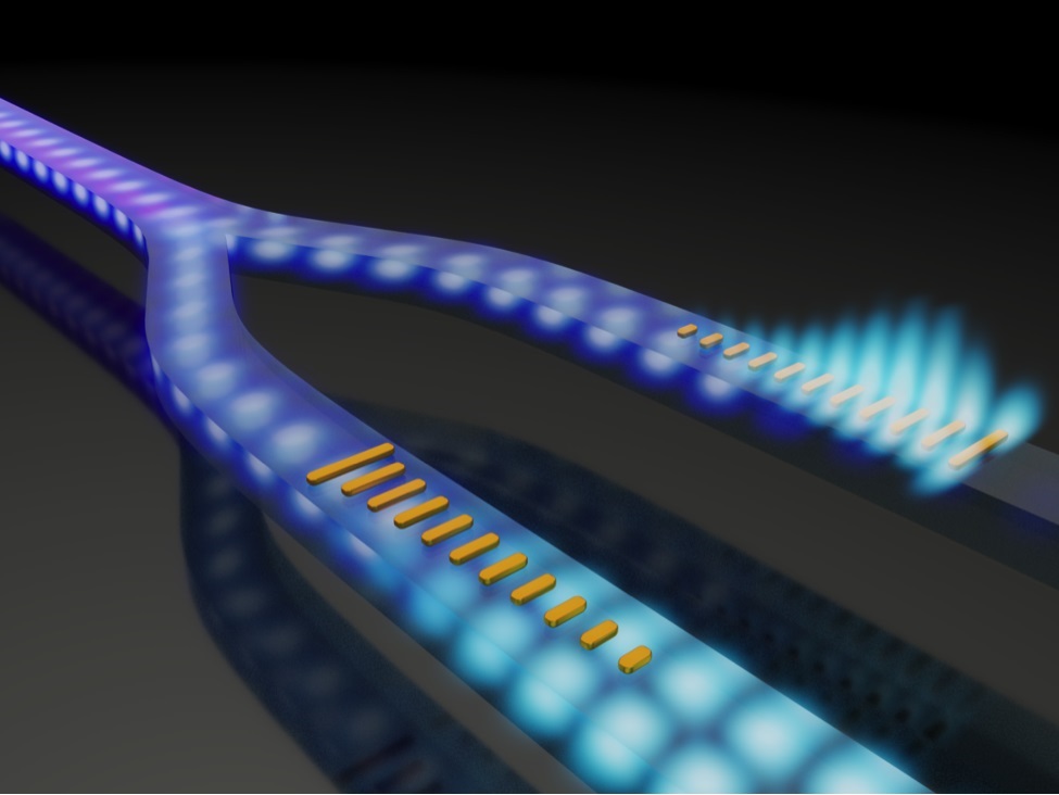
A few realized waveguide mode converters. The devices consist of phased arrays of gold nano-antennas patterned on silicon waveguides. Incident and converted waveguide modes are shown to the left and right of the devices, respectively. Operating wavelength is λ = 4 µm.
—Illustration courtesy of Adam Overvig and Nanfang Yu
Yu’s teams created waveguide mode converters that can convert a certain waveguide mode to another waveguide mode; these are key enablers of a technology called “mode-division multiplexing” (MDM). An optical waveguide can support a fundamental waveguide mode and a set of higher-order modes, the same way a guitar string can support one fundamental tone and its harmonics. MDM is a strategy to substantially augment an optical chip’s information processing power: one could use the same color of light but several different waveguide modes to transport several independent channels of information simultaneously, all through the same waveguide.
“This effect is like, for example, the George Washington Bridge magically having the capability to handle a few times more traffic volume,” Yu explains. “Our waveguide mode converters could enable the creation of much more capacitive information pathways.”
He plans next to incorporate actively tunable optical materials into the photonic integrated devices to enable active control of light propagating in waveguides. Such active devices will be the basic building blocks of augmented reality (AR) glasses—goggles that first determine the eye aberrations of the wearer and then project aberration-corrected images into the eyes—that he and his Columbia Engineering colleagues, Professors Michal Lipson, Alex Gaeta, Demetri Basov, Jim Hone, and Harish Krishnaswamy are working on now. Yu is also exploring converting waves propagating in waveguides into strong surface waves, which could eventually be used for on-chip chemical and biological sensing.
The study is titled, “Controlling Propagation and Coupling of Waveguide Modes Using Phase-Gradient Metasurfaces.” Authors are Zhaoyi Li, Myoung-Hwan Kim, Cheng Wang, Zhaohong Han, Sajan Shrestha, Adam C. Overvig, Ming Lu, Aaron Stein, Anuradha Murthy Agarwal, Marko Lončar, and Nanfang Yu.
The work was supported by the Air Force Office of Scientific Research (grant no. FA9550-14-1-0389, through a Multidisciplinary University Research Initiative program), a Defense Advanced Research Projects Agency Young Faculty Award (grant no. D15AP00111), the National Science Foundation (grant no. ECCS-1307948), and NSF IGERT program (grant no. DGE-1069240). Device fabrication was carried out in part at the Center for Functional Nanomaterials, Brookhaven National Laboratory, which is supported by the U.S. Department of Energy, Office of Basic Energy Sciences (contract no. DE-SC0012704).
The authors declare no competing financial interests.


