04 March 2016
In a recent study published in Nature Communications, ICFO researchers Achim Woessner, Mark B. Lundeberg, Gabriele Navickaite, Davide Janner, led by ICREA Prof at ICFO Frank Koppens and ICREA Prof. at ICFO Valerio Pruneri, in collaboration with CIC nanoGUNE from San Sebastian (Spain), have been able to develop a noninvasive technique capable of efficiently examining the optoelectronic properties of graphene devices at the nanoscale.
Integrating electronic and optoelectronic graphene devices in large scale processing is becoming a reality. However, to achieve a very high device performance of these nanoscale devices, any imperfections at the nanometer or even atomic scale need to be minimized or even eliminated, such as grain boundaries or charge density inhomogeneties or even additional doping near contacts.
The current techniques used for nanoscale device examinantions and characterizations are a major challenge nowadays because they are invasive, need specifically designed device structures, can only image small areas, or even lack the desired nanometer resolution.
Now, the team of researchers has been able to develop a system capable of probing the electrical and optical properties of graphene devices using a technique based on fully non-invasive room-temperature scanning near-field photocurrent nanoscopy. This technique is based on electrical probing of the photoresponse due to strongly localized heating.
The results of this study open a new path for easy, non-invasive, low cost and efficient probing techniques necessary for graphene devices to be integrated in electronic and optoelectronic technologies.
New way of probing graphene devices
ICFO researchers develop a new non-invasive, low cost, room-temperature technique for graphene device characterization.
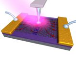
Sketch of Near-field photocurrent technique


