2016/03/31
A Japanese and French international research group, using surface polishing employing light with a controlled direction of oscillation, has for the first time demonstrated that a magnetic field with extremely high frequency (in the petahertz rage. One petahertz corresponds to one trillion oscillation per second) can be used for nanofabrication.
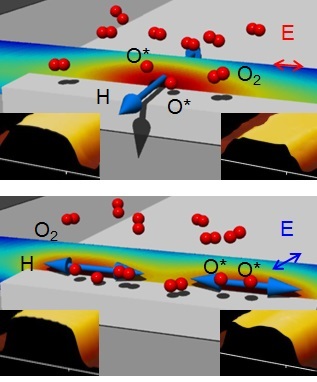
The technology to create nanoscale flat surfaces is essential for the development of electronic devices and optical devices. However, conventional chemical and mechanical polishing methods damage the surface and leave behind impurities. To solve this problem, a University of Tokyo research group developed a non-contact light-based polishing technique called near-field etching that is capable of eliminating surface unevenness. However, it was thought that it was the electric field, not the magnetic field, which contributed to the polishing effect in near-field etching.
The research group of Associate Professor Takashi Yatsui at the University of Tokyo Graduate School of Engineering and Associate Professor Katsuyuki Nobusada at the Institute for Molecular Science and their colleagues examined surface irregularities of zirconia (ZrO2, a transparent material with a high refractive index also known as a type of imitation diamond) during the near-field etching process, and found that the magnetic field determined the properties of the etching process rather than the electric field.
“This discovery revealed that magnetic field oscillating with light frequency can be utilized for fabrication. Although light is an oscillating electric and magnetic field, a magnetic field oscillating with the frequency of visible light does not have any effect on materials. Thus, the effect of the magnetic field was ignored and only the effect of the electric field was considered for applications in light-based fabrication,” explains Yatsui. He continues, “Therefore this is a very surprising result that is in contradiction with what is considered common knowledge. We hope that this discovery will contribute not only to basic research but also to the fabrication of nanostructures for advanced optical and electrical devices.”
This work was partially supported by the JSPS Core-to-Core Program (A. Advanced Research Networks), MEXT Grant-in-Aid (Nos. 26286022, 26630122, 25288012, 15H00866), MEXT Nanotechnology Platform (No.12024046), the HPCI System Research project (ID: hp150218), the Research Foundation for Opto-Science and Technology, and carried out in collaboration with the Institute for Molecular Science, Chuo University, Institute of Materials Science of Mulhouse (IS2M, France), and Université Paris 13 (France).
Paper
T. Yatsui, T. Tsuboi, M. Yamaguchi, K. Nobusada, S. Tojo, F. Stehlin, O. Soppera, D. Bloch, "Optically controlled magnetic-field etching on the nano-scale", Light: Science & Applications Vol. 5, Page number: e16054, doi: 10.1038/lsa.2016.54.
Article link (Publication)


