Hannover, September 24th, 2013
Polymers are often used as an electrically isolating base material for circuit boards. However, miniaturization and extreme stress are pushing the limits of printed circuit boards (PCB) made of epoxy-resin, glass-fiber fabrics (FR4) and polyamides. High temperatures often cause deformation or decomposition of the plastic materials. Due to the thermal expansion characteristics of the materials used, there is subsequently a risk of cracks or breakage in the dielectrical layer. This can, for example, lead to pad cratering, i.e. the formation of craters on the surface of the PCB.
For high temperature applications above 250 °C, thin glass could be a suitable substitute for the conventional polymers used as a basis material for the circuit boards, since glass has a high chemical stability and a low thermal expansion coefficient of 7,2 * 10‑6 K‑1. The field of aerospace technology has interesting applications for these new, thin glass circuit boards.
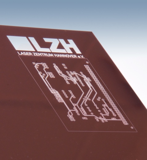
Together with project partners, the Laser Zentrum Hannover e. V. (LZH) is developing production processes for multilayer circuit boards based on thin glass with 145 µm thicknesses. The trend to miniaturization and higher processing speeds in the PCB industry is a special challenge for manufacturing. In the “Glass PCB Project”, scientists in the Glass Group of the Production and Systems Department are working on developing two different laser processes for processing these special materials: First, a laser is used to structure the metal layers. According to the PCB layout, a laser is used to make conducting tracks by removing excess metal from a thin glass base. The advantages of laser ablation are especially apparent in the extremely fine structural resolution of the metal, without causing damage to the sensitive material.
Secondly, a laser is used to form holes or vias to connect the different circuit board layers, or the conventional components. The LZH is currently working on finding suitable laser parameters to drill through the materials without causing thermal damage. Also, the vias should be of high quality, and be reproducible at high speeds. Optimal results aim at generating parallel vias through the glass layers. The process time, which is dependent on the material thickness and the circuit board layout, is presently 2 s for drilling a microvia with a 0.2 mm diameter through a 170 µm thick material, with a tendency towards shorter times.
Also, comparative investigations carried out by project partner TU Berlin (main area of research – Technologies for Micropherics) show that new material systems based on thin glass must use the laser for drilling vias, since conventional, mechanical drilling causes unwanted microcracks, and the service life of the drills is 40 times shorter.
Altogether, three scientific institutes and four industrial companies are involved in the joint project. The LZH develops the laser processes for structuring the circuit board layouts and for drilling the vias, and the industrial partners such as Schott AG provide thin glass materials. The circuit board manufacturer Hotoprint GmbH & Co. KG offers both production processes for the thin glass circuit boards and electroplating. KCS Europe GmbH is in charge of coating technologies (sputtering) of the conducting metal layers on the thin glass. Furthermore, CCI Eurolam GmbH is involved as a specialist for materials for circuit board manufacturing. Process handling of the thin glass sheets for multilayer boards is being researched by the Institute of Transport and Automation Technology (ITA) of the University of Hannover.
The project “Glass PCB – Development of a Multilayer Circuit Board Based on Thin Glass” will be funded by the Central Innovation Program SME (ZIM) of the Federal Ministry of Economics and Technology (BMWi) until the middle of 2014.


