MINNEAPOLIS / ST. PAUL (09/03/2013) — international group of researchers from the University of Minnesota, Argonne National Laboratory and Seoul National University have discovered a groundbreaking technique in manufacturing nanostructures that has the potential to make electrical and optical devices smaller and better than ever before. A surprising low-tech tool of Scotch Magic tape ended up being one of the keys to the discovery.
The research is published today in Nature Communications, an international online research journal.
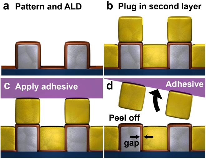
Combining several standard nanofabrication techniques—with the final addition of the Scotch Magic tape—researchers at the University of Minnesota created extremely thin gaps through a layer of metal and patterned these tiny gaps over the entire surface of a four-inch silicon wafer. The smallest gaps were only one nanometer wide, much smaller than most researchers have been able to achieve. In addition, the widths of the gaps could be controlled on the atomic level. This work provides the basis for producing new and better nanostructures that are at the core of advanced electronic and optical devices.
One of the potential uses of nanometer-scale gaps in metal layers is to squeeze light into spaces much smaller than is otherwise possible. Collaborators at Seoul National University, led by Prof. Dai-Sik Kim, and Argonne National Laboratory, led by Dr. Matthew Pelton, showed that light could readily be squeezed through these gaps, even though the gaps are hundreds or even thousands of times smaller than the wavelength of the light used. Researchers are very interested in forcing light into small spaces because this is a way of boosting the intensity of the light. The collaborators found that the intensity inside the gaps is increased by as much as 600 million times.
"Our technology, called atomic layer lithography, has the potential to create ultra-small sensors with increased sensitivity and also enable new and exciting experiments at the nanoscale like we’ve never been able to do before," said Sang-Hyun Oh, one of the lead researchers on the study and a professor of electrical and computer engineering in the University of Minnesota’s College of Science and Engineering. "This research also provides the basis for future studies to improve electronic and photonic devices."
One of the most surprising outcomes of the research is that Scotch Magic tape was one of the keys to the discovery. Etching one-nanometer-wide gaps into metals is not feasible with existing tools. Instead, the researchers in Oh’s team constructed the nano-gaps by layering atomic-scale thin films on the sides of metal patterns and then capping the structure with another metal layer. No expensive patterning tools were needed to form the gaps this way, but it was challenging to remove the excess metals on top and expose the tiny gaps. During a frustrating struggle of trying to find a way to remove the metal films, University of Minnesota Ph.D. student and lead author of the study Xiaoshu Chen found that by using simple Scotch Magic tape, the excess metals could be easily removed.
"The Scotch tape works nicely, which was unexpected," said Oh. "Our technique is so simple yet can create uniform and ultra-small gaps like we’ve never been able to do before. We hope that it will rapidly be taken up by many researchers."
In addition to Oh and Chen, researchers involved in the study include a joint lead author Hyeong-Ryeol Park, who was a Ph.D. student at Seoul National University and is now a postdoc in Oh’s group at the University of Minnesota; Matthew Pelton, a staff physicist at Argonne National Laboratory who is now a professor of physics at the University of Maryland, Baltimore County; Nathan Lindquist, a former Ph.D. student at the University of Minnesota who is now a professor of physics at Bethel University in St. Paul; Hyungsoon Im, a former electrical and computer engineering Ph.D. student who is now a postdoc at Harvard Medical School; and Xianji Piao, Yun Jung Kim, Jae Sung Ahn, Kwang Jun Ahn, Prof. Namkyoo Park, and Prof. Dai-Sik Kim, all from Seoul National University in Korea.
This research was funded by the U.S. Department of Defense (DARPA Young Faculty Award and the ONR Young Investigator Program), the U.S. Department of Energy and the National Research Foundation of Korea with capital equipment funding from the Minnesota Partnership for Biotechnology and Medical Genomics.
To read the full research paper entitled, "Atomic layer lithography of wafer-scale nanogap arrays for extreme confinement of electromagnetic waves," visit the Nature Communications website.
Related Links
College of Science and Engineering: http://cse.umn.edu/index.php
Nature Communications: http://www.nature.com/ncomms/2013/130903/ncomms3361/full/ncomms3361.html