Tokyo and Kawasaki, Japan, October 17, 2013 — Fujitsu Limited and Fujitsu Laboratories Ltd. today announced development of a high-sensitivity receiver chip that will pave the way to high-capacity, gigabit-capable wireless devices operating at 240GHz in the millimeter-wave frequency band.
The 240GHz band is a frequency range over 100 times wider than that used by typical mobile devices today (0.8–2GHz), which should enable a 100-fold increase in communications capacity. To achieve such an increase, however, requires amplifiers with high amplification ratios that can receive signals that have become very faint when transmitted through the air.
Given this, Fujitsu and Fujitsu Laboratories have developed a technology for multistage amplifiers that increases amplification ratios while suppressing an amplifier's oscillator effect, and a technology that efficiently transmits the amplifier's output signal to the next stage. The result is that the receiver chip's sensitivity is increased roughly tenfold, making possible the reception of large data volumes by smartphones or other mobile devices using a compact antenna.
A portion of these research results were obtained through "R&D Program on Multi-tens Gigabit Wireless Communication Technology at Subterahertz Frequencies," a research program commissioned by Japan's Ministry of Internal Affairs and Communications as part of its "Research and Development Project for Expansion of Radio Spectrum Resources."
Details of this technology are being presented at CSICS 2013, the Compound Semiconductor IC Symposium, opening October 13 in Monterey, California.
Background
The explosive growth of smartphones and other wireless devices has brought about an increase in the use of mobile data communications for browsing the web or downloading music, alongside conventional voice communication. With an expected shift toward high-capacity data communications, including videos and movies, there is an expectation that demand will grow for devices that can instantly download such data. In order for that to happen, high-capacity wireless devices will need to use wider frequency ranges than they do now. Wireless devices that could use millimeter-wave frequencies would be able to take advantage of a frequency range 100 times wider than that used by today's wireless devices, so it is expected that they would also be able to handle communications speeds 100 times greater.
Millimeter-wave transmissions, particularly at such high frequencies as 240GHz, however, become severely attenuated as the radio waves travel through the air. Receiving such a faint signal requires a highly sensitive receiver (comprised of an antenna, amplifier, and wave detector). The introduction of an amplifier with a high amplification ratio shows has been sought after as an effective way of improving reception sensitivity.
Technological Issues
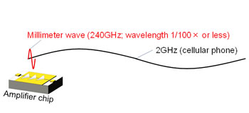
A common way of increasing the amplification ratio of the amplifier is to connect multiple amplifiers as part of a staged construction, but more stages result in bigger chip sizes. When applying this technique in the 240GHz band, the wavelength of the signal is very short – less than 1 mm – so the length can be shorter than the chip itself (Figure 1). This creates technical problems that do not exist at the frequencies used by today's cellular phones (that use the 2GHz band). Output signals from the amplifier can leak to ground on the chip's surface, and these leaked signals return to the amplifier's input pin, resulting in double amplification (Figure 2). When the leaked signal re-enters the amplifier, it is amplified again and produces even more signal leakage, which returns to the input pin yet again, creating what is known as the oscillator effect, making it difficult to receive these signals correctly. For this reason, creating a high amplification ratio with millimeter waves requires a technology that can suppress these oscillations without losing amplification levels.
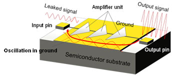
Figure 2: Signal leakage through ground
About the New Technology
Building on indium phosphide high electron-mobility transistor (InP HEMT) technology developed by Fujitsu Laboratories, Fujitsu and Fujitsu Laboratories developed a multistage amplifier that suppresses the oscillator effect while increasing the amplification ratio. Also developed was an impedance-matching technology that efficiently conveys the output signal from one stage to the next. This produces a roughly tenfold improvement in receiver-chip sensitivity over previous designs. Key features of the technology are as follows.
1. Multistage amplifier suppresses oscillator effect, increases amplification ratio
The leaked signal from an amplifier will always have "antinodes" at specific sites where that signal is at its greatest amplitude, and "nodes" where it has no amplitude at all. If the amplifier's input pin is located in a leaked signal's antinode, then a stronger leaked signal will feed back into the amplifier, creating the oscillation effect (Figure 3, top). Conversely, if the input pin is located in a node, the leaked signal has no amplitude, and the amplifier will not re-amplify the leaked signal. Fujitsu has aligned the input pin and output pin with the nodes in the leaked signal (Figure 3, bottom). Connecting amplifiers designed this way into multiple stages results in high amplification ratios without an oscillator effect.
2. Impedance-matching technology efficiently transmits amplifier output signal to next stage
Efficiently transmitting the output signal from an amplifier to the next stage requires impedance matching on the lines that connect the amplifiers, which, in turn, requires that the lines be of a uniform length. But aligning the input and output pins of the amplifiers with the nodes limits the dimensions of the amplifier, while the length requirements on the lines create another set of constraints, complicating the task of impedance matching. To resolve this problem, a U-shaped line was deployed and the length and width of the U were adjusted to enable impedance matching regardless of the limitations on the dimensions of the amplifier.
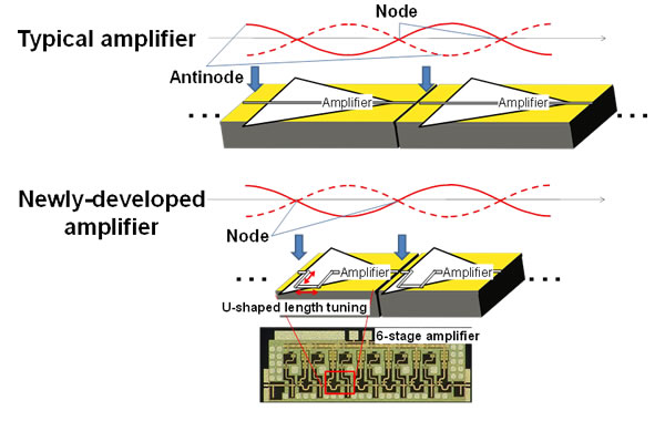
Figure 3: A conventional amplifier and the newly-developed amplifier
Results
These technologies have produced a roughly tenfold improvement in the sensitivity of a receiver chip compared with previous designs. These receivers could be used in smartphones and other wireless devices equipped with compact antennas. And because this would also allow for antennas with broader relative directionality than existing devices, there would be no need to precisely align the transmitter to the handset (Figure 4), resulting in greater convenience for users.
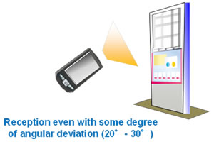
Figure 4: Scenario showing handset in use
Future Plans
Fujitsu is working to develop a compact package that integrates an antenna along with a receiver chip based on this technology, with the goal of conducting transmission testing by sometime in 2015 and practical applications around 2020.