April 7, 2014
PML researchers have developed a novel method of fabricating graphene-based microdevices that may hasten the arrival of a new generation of standards for electrical resistance. The new design offers substantial performance enhancement over most existing devices, and can be adjusted to produce a wide range of electronic properties.
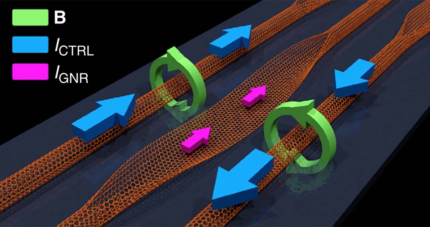
Since 1990, the internationally accepted means of realizing the ohm has been based on the quantum Hall effect* (QHE), in which resistance is exactly quantized in increments dictated by constants of nature. The QHE is measured using electrical contacts placed along the sides of a rectangular, cryogenically cooled, current-bearing conductor (the “Hall bar”) in which the charge carriers behave like a two-dimensional (2D) gas.
Charge carriers then condense at one or more energy levels in a strong magnetic field, and this produces resistance plateaus. The widely-used standards for such measurements are based on GaAs/AlGaAs heterostructure devices and require high magnetic field strengths in the range of 5 tesla (T) to 15 T, typically obtainable only with expensive superconducting magnets.
When QHE was first observed in graphene ten years ago, the inherently 2D material became a prime candidate for realizing the quantized Hall resistance (QHR) standard because QHE plateaus could be observed in graphene at lower magnetic field strength and higher temperature than in semiconductor devices.
In general, there are three ways to obtain monolayer graphene sheets suitable to that task: the sticky-tape “exfoliation” method used in 2004 to isolate the material for the first time; chemical vapor deposition on copper or other material; and growth on an insulating silicon carbide substrate, which the PML researchers employ.**
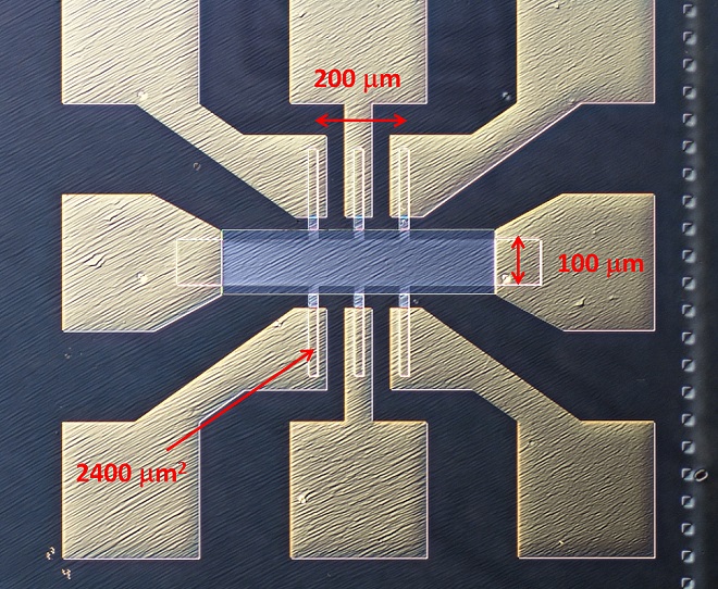
No matter how it is obtained, however, incorporating graphene into a practical standard entails the same sort of lithographic techniques used to fabricate most microstructures: features are created by spin-coating a polymer-based liquid over a surface, drying it, and exposing certain regions of the sample to light or to an electron beam to form masks for etching.
“There are serious difficulties when working on graphene in that environment,” says physicist Rand Elmquist of the Quantum Measurement Division. “Being an open surface, graphene is very sensitive to chemicals in the air or from materials it contacts. In normal photolithography or electron-beam lithography, the fabrication process lays down organic compounds – the liquid resist – onto whatever material is being treated. Those organic compounds leave a residue on graphene that won’t come off, creating imperfections in surfaces and contacts that can affect the electronic behavior.
“So we came up with a new way to make devices that we hoped would produce better contacts, and also keep the graphene clean, and free of organic contamination.”
This method, developed at PML by physicist Yanfei Yang involves coating a sheet of graphene on a section of silicon carbide wafer with about 15 nanometers of gold before any lithography. Patterns are developed using traditional photolithography to remove any unwanted gold-coated graphene. Then, the areas that will be the Hall bar contacts get a thicker coating of gold, so that they will make good connections for wires used in electrical measurements. In the last step, the gold layer over the area of graphene that will serve as the Hall bar is removed with dilute aqua regia, a mixture of nitric acid, hydrochloric acid, and deionized water, leaving the graphene almost completely clean.
“To our surprise,” says Elmquist of the Fundamental Electrical Measurements Group, “we found that aqua regia etching produces helpful p-type doping in the graphene.” That is, molecules from the acids stick to the surface, reducing the carrier density and improving the mobility of electrons that remain. Low carrier density is important because the higher the density of charge-carriers in the Hall bar, the higher the magnetic field strength required to observe the critical QHE plateaus.
“Normal epitaxial graphene (EG) grown on SiC has an electron density of 1013 per square centimeter,” Elmquist says. “At that level, you can’t see the QHE”; doing so would require a magnetic field strength far too high to be used in a working standard. “As a practical matter, you need to get down to around 5 x 10¹¹ per cm2 or lower for use at reasonable field strength.”
By contrast, the PML group’s new EG devices were shown to have carrier densities in the range of 3 x 10¹⁰ per cm2 to 3 x 10¹¹ per cm2, allowing observation of clearly defined resistance quantization at magnetic field strengths of less than 4 T. The p-type molecular doping effect can be reduced by heating in argon gas, and is restored by dipping in aqua regia.
The team has submitted its results for publication in the journal Advanced Materials. But there is much more to learn. “One thing we are working on is a better understanding of how the QHE develops in graphene, and specific features of the QHE that occur nowhere else” Elmquist says; “One day soon we hope to implement this or a similar method to make nearly perfect graphene QHR devices that surpass the best grown with GaAs.”
* The Hall effect occurs when current traveling through a conductor is exposed to a magnetic field oriented at a 90-degree angle to the current flow. Because of the effect of the field on the charge carriers, electron (or hole) populations are higher on one side of the conductor and lower on the other. This produces a transverse voltage that is perpendicular to both the current flow and the field. At the quantum level, the effect is exactly quantized, and resistance – as determined by the ratio of transverse voltage to current – is thus also quantized.
** The PML group makes epitaxial graphene (EG) by heating a crystal of SiC to as high as 2100 ͦC. Silicon on the outermost surface turns to gas. The remaining carbon atoms arrange themselves into hexagonal units and form a sheet of graphene atop and aligned with the underlying crystal. The EG process has advantages for making devices compared to the other two familiar sources of graphene. Exfoliation of graphite produces sheets with dimensions in the range of tens of micrometers – too small for many uses. And graphene grown by chemical vapor deposition has to be removed from its metal substrate and transferred elsewhere, whereas EG can be used as formed. One drawback to the technique is that the EG layers are doped by the formation of covalent bonds with the underlying crystal and have high electron densities.
The collaboration includes researchers now at Georgetown University and institutions in Japan, Taiwan, and Argentina.