November 20, 2014
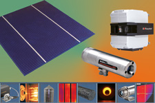
Berlin – Raytek and Ircon pyrometers ensure exact temperature monitoring of all processes in the production of photovoltaic cells and modules. Noncontact measurement of the infrared radiation is an ideal solution especially for high-temperature processes, difficult-to-access measuring points such as vacuum chambers, and for products that must not be contaminated or mechanically damaged.
The comprehensive sensor portfolio of both brands enables the implementation of a long-term stable temperature control as well as the efficient use of energy and valuable resources. In polycrystalline silicon production (Siemens process), high-performance pyrometers with a variable focus and very small measurement spots monitor the temperature of the slowly growing rods for days. They are unaffected by interferences such as contamination of the process reactor window and thus ensure high reliability. Since the atmosphere contains hydrogen, the pyrometers are enclosed in special explosion-proof housings.
There are different established processes for monocrystalline silicon production. In each case, the melt temperature must be monitored. Glass-fiber pyrometers are the optimal solution for the float-zone method as they detect even very small targets and are resilient against electromagnetic interferences from the induction heater.
Single-crystal silicon production by means of the Czochralski process is best controlled with ratio pyrometers which in addition to the melt temperature also monitor the boule diameter. Pyrometers are furthermore used to ensure that the wafer temperature does not exceed 25 °C during polishing. Through-the-lens viewing enables operators to precisely aim the sensor at critical locations on the wafer.
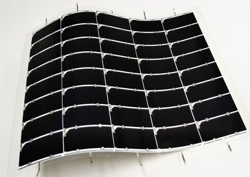
In thin-film PV cell manufacturing, high-resolution thermal imagers monitor the even temperature of the substrate and the film, thereby ensuring clean, void-free deposition. Thermal imagers (matrix cameras) or infrared linescanners, which record thermal images of moving processes, are employed for functional testing of the completed PV modules. All systems are designed for a simple integration into existing facilities. They include powerful software with application-specific functions. Process parameters can be precisely and directly controlled via sensor outputs.
Source:

