December 4, 2013
Researchers from the NIST Center for Nanoscale Science and Technology (CNST) have demonstrated a new low energy electron beam technique and used it to probe the nanoscale electronic properties of grain boundaries and grain interiors in cadmium telluride (CdTe) solar cells. Their results suggest that controlling material properties near the grain boundaries could provide a path for increasing the efficiency of such solar cells.
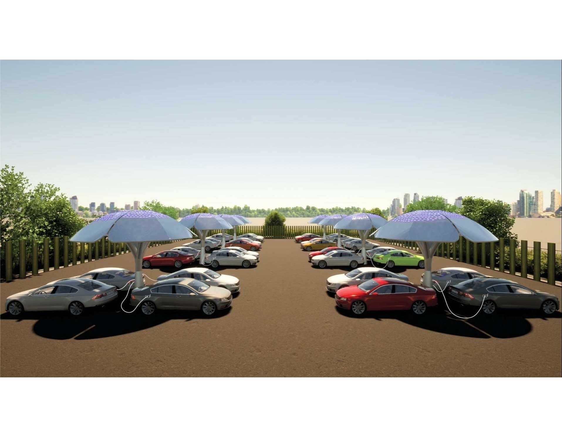
Among thin film photovoltaic solar cells, those made from cadmium telluride are some of the most successful on the market. However, the efficiency of commercial cells is still less than half of the theoretical maximum, and the underlying mechanisms for the deficiency are not well understood. CdTe cells are believed to lose current at their material grain boundaries; however, it has also been suggested these grain boundaries have properties that could actually improve carrier collection if they were better understood.
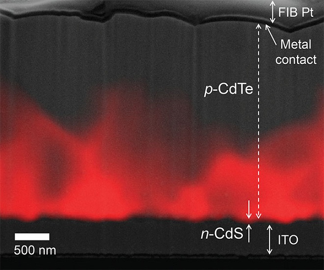
Characterization techniques using focused electron beams to induce currents are increasingly used for investigating the properties of thin film solar cells. The measurements are easier using high energy electrons, but the higher energy reduces the spatial resolution. The researchers extended traditional electron-beam-induced current measurements by using low energy beams to locally excite the CdTe and create current. These beams have a spatial resolution of about 20 nm, small enough to map the photocurrent response inside the grain interiors or at the grain boundaries.
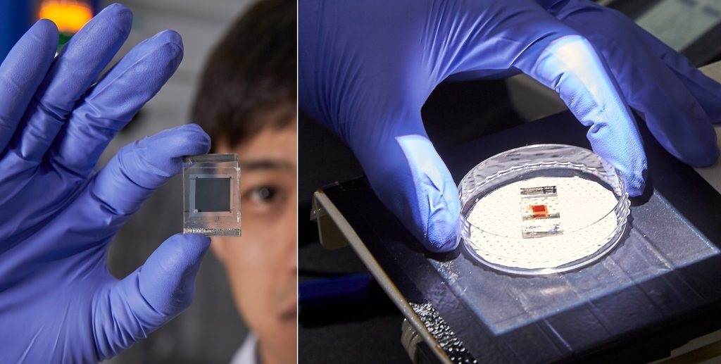
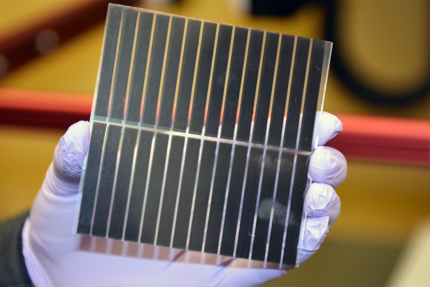
The measurements were performed on fragments extracted from a commercial thin film solar cell. Nanoscale electrical contacts were prepared with sizes comparable to a single or a few grains, confining the current path to sizes relevant for understanding current production and loss.
The measurements show that a large fraction of grain boundaries display higher current collection than the grain interiors, seemingly enhancing device performance. However, using 2D finite element simulations, the researchers demonstrated that these grain boundaries also create a large pathway for leakage current, which completely negates the efficiency gains from the enhanced photocurrent collection.
The researchers believe that their technique provides a valuable tool for visualizing the behavior of photovoltaic cells at the length scales needed to understand both loss mechanisms within photovoltaic materials as well as internal structures within these materials that may lead to higher overall cell efficiencies.
*Local electrical characterization of cadmium telluride solar cells using low-energy electron beam, H. P. Yoon, P. M. Haney, D. Ruzmetov, H. Xu, M. S. Leite, B. H. Hamadani, A. A. Talin, and N. B. Zhitenev, Solar Energy Materials and Solar Cells 117, 499-504 (2013).