Kawasaki, Japan, and Beijing, China, March 22, 2016: Fujitsu Laboratories Ltd. and Fujitsu R&D Center Co., Ltd. (collectively "Fujitsu") today announced that, to connect multiple datacenters scattered within a metropolitan area with high capacity and at low cost, they have developed a basic architecture for digital-signal processing in optical transceivers transmitting data at 400 gigabits per second over a single wavelength.
Fujitsu have developed new transceiver architecture in which, on the transmitter side, a specially designed reference signal is transmitted, and this is used on the receiving end to effectively compensate for distortion. Fujitsu successfully performed repeaterless transmission tests over a distance of 160 km. This technology accurately compensates for variations in the characteristics of transceiver components and distortions introduced in the transmission path, making it possible to communicate at 400 Gbps per wavelength using inexpensive optical transceiver components.
This technology can be applied to integrated optical transceiver components using silicon photonics, a technology expected to reduce costs and contribute to building next-generation distributed computing platforms that will support 5G mobile networking and diverse IoT services.
As 5G mobile networks and the IoT advance, over the next few years it is expected that an era will arrive in which users can access ever more devices and data volumes while enjoying a greater level of real-time services. To achieve that, development work is advancing on distributed computing platforms, in which multiple datacenters are distributed throughout a metropolitan area and connected to work together (Figure 1). There is a need for the fiber-optic networks that will tie these datacenters together to carry more bandwidth, and now R&D activities are underway to go from currently common speeds of 100 Gbps per wavelength, up to 200 Gbps and eventually 400 Gbps.
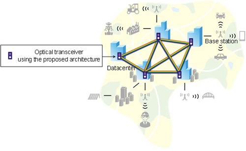
Figure 1: A metropolitan area data center network implementing a distributed computing platform
Until now, achieving 400 Gbps per wavelength has required the use of expensive components that have been optimized and selected for specific purposes. While there are expectations that the price of components for optical transceivers could be brought down by using cheaper parts or by using CMOS technology or silicon photonics technology, which are being developed in parallel, these all have relatively poor performance compared to expensive components that have been optimized and selected for the specific purpose. Due to piece-to-piece performance variations of the components, economically transmitting over distances of roughly 100 km, the distance needed for communications between datacenters, has not been possible using current methods.
To enable cost savings in optical transceivers, Fujitsu has developed a new optical transceiver architecture in which the receiver compensates for distortions, particularly those from transmitters that are expected to significantly degrade performance.
In this architecture, on the transmitter side, a reference signal that will remain relatively unaffected by the transmitter's own signal distortions along the transmission path is combined with the data signal. This combined signal is then sent, and the receiver can then effectively compensate for the transmitter's signal distortion (Figure 2).
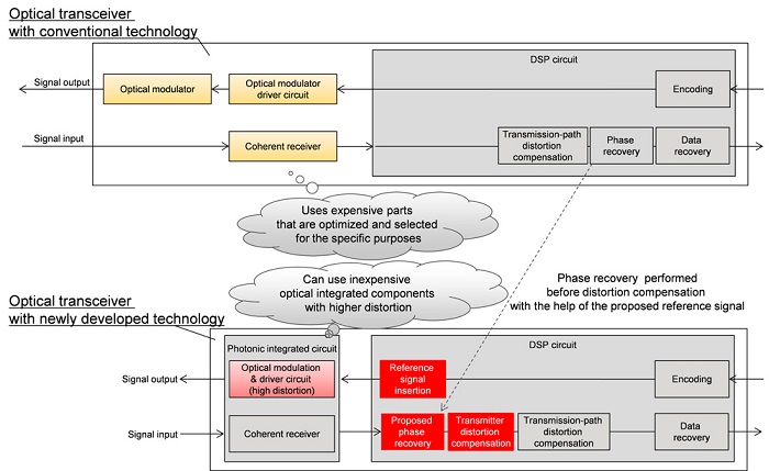
Figure 2: Optical transceiver block diagram
The typical approach used up to now has been to observe the output signal of the transmitter and compensate for signal distortions there in order to have the transmitter provide the highest quality signal possible. But when transmitting at 400 Gbps, the desired processing accuracy becomes very high, so it is difficult to compensate on the transmitter's end without significant increase of costs for components and circuits. Fujitsu has developed a new architecture in which, by transmitting a specially designed reference signal, it is possible to compensate for the transmitter's signal distortion on the receiver's end.
Fujitsu successfully tested this technology to transmit data at 400 Gbps over fiber optic lines across 160 km, regarded as a sufficient distance for a wide-area network between datacenters in a metropolitan area (Figure 4). Furthermore, this technology can be applied to compensate for variations in performance when using low-cost components, which has been a problem. These results demonstrate that it will be possible to build a next-generation distributed computing platform using low-cost transceivers that operate at 400 Gbps per wavelength.
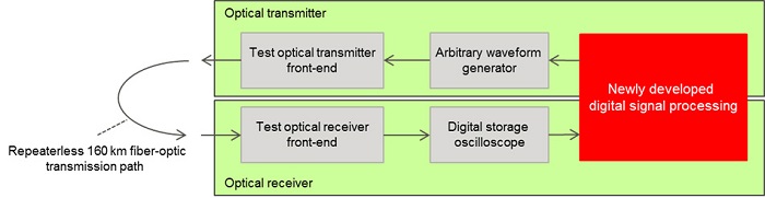
Figure 4: Configuration of 160 km repeaterless transmission test setup using this technology