March 11, 2015
WASHINGTON—Today's explosion of video and Internet data is driving unprecedented traffic demand within datacenters. With data transfer rates exceeding 100 gigabits-per-second (Gb/s), communication between servers requires optical switches with faster switching time (micro-to nano-second level), broader band operation, larger capacity for switching elements and lower energy consumption.
Researchers at the University of California, Berkeley have developed a novel silicon photonic switch, which is the largest-scale and the lowest-energy loss switch reported to date. It features a switching time of sub-micro seconds and a broad bandwidth of hundreds of nanometers.
The researchers will present their photonic switching innovation on 23 March 2015 during the Optical Fiber Communication Conference and Exposition (OFC) in Los Angeles, California, USA. A step forward towards achieving large-scale silicon photonic switches for high-traffic datacenter networks, the new device will boost other technologies that rely on manipulating multi-channel optical signals, such as secure communications and quantum computing.
"Our photonic switch has 50 input and 50 output channels, for a total of 2,500 switching elements located on the cross points of these channels, which is the largest-scale silicon photonic switch ever reported," said Tae Joon Seok, a postdoctoral researcher at the Integrated Photonics Laboratory at the university. "The switch can be compactly integrated on a silicon chip smaller than 1 cm x 1 cm."
Seok said that the largest-scale silicon photonic switch previously reported by other groups has 8 input and 8 output channels.
The Role of Photonic Switches in a Network
In an optical communications network, optical switches reconfigure the path of optical signals transmitted on integrated optical circuits, enabling signals to be selectively switched from one circuit to another. The major barrier limiting switch scale is the cumulative optical losses caused by switch architecture. This new breakthrough is significant, Seok added, because increasing the scale or the number-of input and output channels of optical switches provides larger capacity for the network to process optical signals.
Regular silicon photonic switches consist of a number of smaller optical switcheswith one or two input and output channels (1x2 or 2x2) as switch elements. These elements are cascaded with each other to form a two-dimension switching network. When optical signals are transmitted in the network,the light undergoes energy losses accumulated as it goes through multiple switching elements, and because these switching elements cannot transfer 100 percent of light energy, the size of switches are limited.
"Generally, the light energy loss, or technically called optical insertion loss, is quickly added up as the scale of the switch increases," Seok said. "To compensate for the loss, optical amplification is required, which increases power consumption used by the switch. This, in turn, increases the overall price per switch."
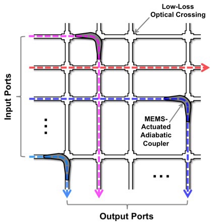
To address this problem, Seok and his co-workers designed a new switch architecture that enables scalability. Rather than connecting smaller optical switches in succession to form a switching network, the new architecture is a single-stage switch with a MEMS switching mechanism, which completely eliminated the problem of cumulative loss.
According to Seok, he and his colleagues first patterned a bottom silicon layer to create the east-to-west input and north-to-south output channels. Then, with the aid of a sacrificial spacer layer, a top silicon layer was built on and patterned to form a specific type of switching element, called an adiabatic coupler. An adiabatic coupler is a gradually tapered waveguide, which transfers light from one channel to another channel without wavelength dependency.
When the switch is in the "on" mode, adiabatic couplers on the top layer are pulled down to bottom channels, transferring light and making 90 degree turns from the input channel to the output channel. When the switch is in the "off" mode, the light stays in the input channel and is not affected by the switching elements due to the distance between the top and bottom layers.
"In this architecture, light from each input port would only pass one switching element in their light paths rather than passing multiple ones like in conventional silicon switch, which greatly reduces the energy losses," Seok explained.
Moreover, in the "switch-off" mode, light propagating in the bottom layer channels would stay in the channel without disturbance from switching elements, thus reducing energy loss. As a result, the energy loss of the newly designed switches per port is three times lower than conventional switches.
Seok said the novel switch architecture is highly scalable, possibly allowing switches larger than 100x100 ports fabricated on a tiny chip. The newly designed switch also features hundreds of nanometers of bandwidth, which is about 10 times broader than that of regular silicon switches and provides larger capacity for the network to process information.
"Although commercially available [devices] like 3D-MEMS optical switches can also have up to hundreds of input/output ports and low energy loss, the switch speed is slow, around millisecond level, and the physical size is large," Seok said.
"Our switch features sub-microsecond switching time, which is three orders of magnitude faster than 3D-MEMS switches. Also, the new switch is based on silicon photonics and can be implemented on a tiny silicon chip less than 1 cm x 1 cm, which may reduce the manufacturing costs and enable a low-cost mass production."
This work is a crucial step forward towards achieving large-scale silicon photonic switches for high-traffic datacenter networks, but is also applicable to any area that requires manipulation of multi-channel optical signals, such as secure communications and quantum computing.
The researchers' next step is to further reduce the energy loss for real manufacturing production and integrate the switch with the electronic driving circuit in optical communication network.
About the Presentation
The presentation, "50x50 Digital Silicon Photonic Switches with MEM-Actuated Adiabatic Couplers," by Tae Joon Seok, Niels Quack, Sangyoon Han, Ming C. Wu, will take place at 14:30, Monday, 23 March 2015, in Room 403A at the Los Angeles Convention Center, Los Angeles, California, USA.