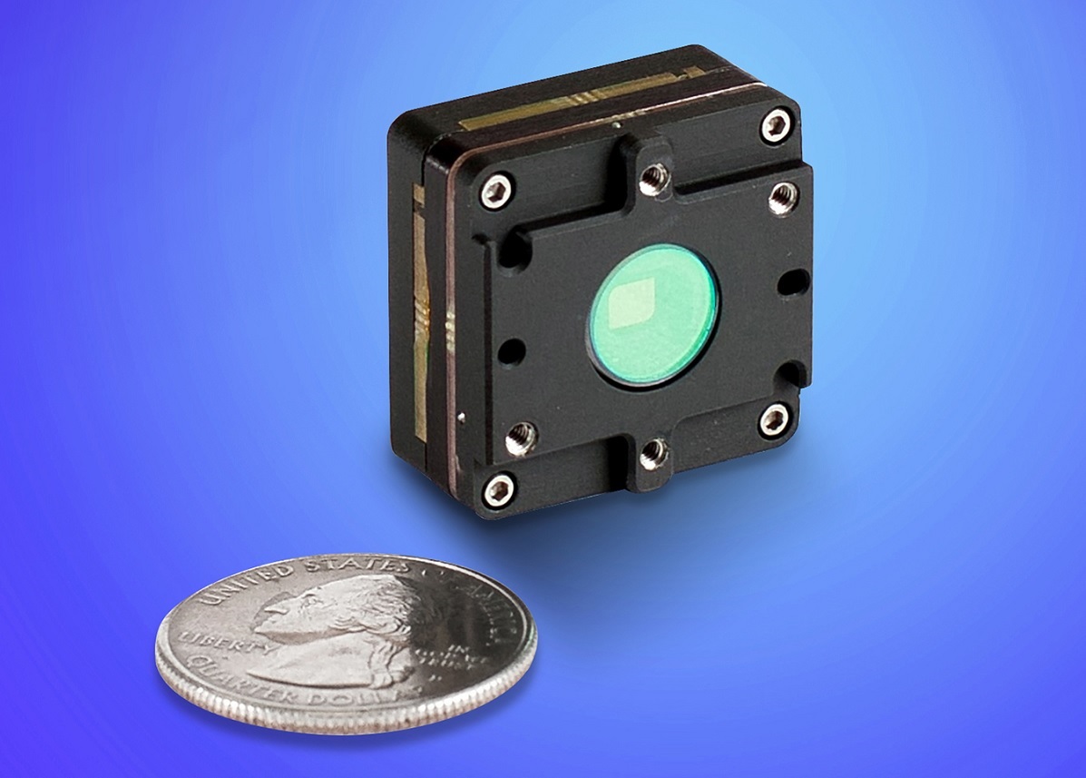
Tokyo, Japan—Sony Corporation today announced that it has developed a 1.46 effective megapixel back-illuminated CMOS image sensor equipped with a Global Shutter function*1. The newly developed pixel-parallel analog-to-digital converters provide the function to instantly convert the analog signal from all pixels, simultaneously exposed, to a digital signal in parallel. This new technology was announced at the International Solid-State Circuits Conference (ISSCC) on February 11, 2018 in San Francisco in the United States.
CMOS image sensors using the conventional column A/D conversion method read out the photoelectrically converted analog signals from pixels row by row, which results in image distortion (focal plane distortion) caused by the time shift due to the row-by-row readout.
The new Sony sensor comes with newly developed low-current, compact A/D converters positioned beneath each pixel. These A/D converters instantly convert the analog signal from all the simultaneously exposed pixels in parallel to a digital signal to temporarily store it in digital memory. This architecture eliminates focal plane distortion due to readout time shift, making it possible to provide a Global Shutter function*1, an industry-first for a high-sensitivity back-illuminated CMOS sensor with pixel-parallel A/D Converter with more than one megapixel.
![]()
The inclusion of nearly 1,000 times as many A/D converters compared to the traditional column A/D conversion method means an increased demand for current. Sony addressed this issue by developing a compact 14-bit A/D converter which boasts the industry's best performance in low-current operation.
Both the A/D converter and digital memory spaces are secured in a stacked configuration with these elements integrated into the bottom chip. The connection between each pixel on the top chip uses Cu-Cu (copper-copper) connection*5, a technology that Sony put into mass production as a world-first in January 2016.
In addition, a newly developed data transfer mechanism is implemented into the sensor to enable the high-speed massively parallel readout data required for the A/D conversion process.
![]()
Left: cross-section of the Cu-Cu connection, Upper right: pixel substrate, Lower right: logic substrate
Global Shutter function achieved in a high-sensitivity back-illuminated CMOS image sensor by using the following key technologies:
- Low-current, compact pixel-parallel A/D converter
In order to curtail power consumption, the new converter uses comparators that operate with subthreshold currents, resulting in the industry's best-performing*4, low current, compact 14-bit A/D converter. This overcomes the issue of the increased demand for current due to the inclusion of nearly 1,000 times as many A/D converters in comparison with the traditional column A/D conversion method.
- Cu-Cu (copper-copper) connection
To achieve the parallel A/D conversion for all pixels, Sony has developed a technology which makes it possible to include approximately three million Cu-Cu (copper-copper) connections in one sensor. The Cu-Cu connection provides electrical continuity between the pixel and logic substrate, while securing space for implementing as many as 1.46 million A/D converters, the same number as the effective megapixels, as well as the digital memory.
- High-speed data transfer construction
Sony has developed a new readout circuit to support the massively parallel digital signal transfer required in the A/D conversion process using 1.46 million A/D converters, making it possible to read and write all the pixel signals at high speed.