June 05, 2017
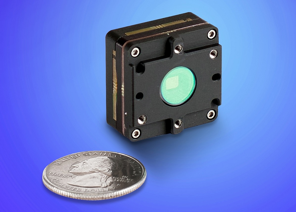
Tokyo, Japan — Sony Corporation ("Sony") today announced it has developed a back-illuminated time-of-flight ("ToF") image sensor with a 10µm pixel pitch, the industry's smallest. This accomplishment was made possibly combining the ToF image sensor technology of Softkinetic Systems S.A. ("Softkinetic"), a Sony subsidiary acquired in 2015, and Sony's back-illuminated CMOS image sensor technology. Research results on the sensor were made public at the "2017 Symposia on VLSI Technology and Circuits" on Monday, June 5, 2017 in Kyoto, Japan.
With ToF technology, the distance to an object is measured by the time it takes for light from a light source to reach the object and reflect back to the sensor. ToF image sensors detect distance information for every pixel, resulting in highly accurate depth maps. Accuracy can be enhanced even further by ensuring that the reflected light is efficiently received and that the processing required to measure distance is executed at a high frame rate. Additionally, power consumption can be reduced by efficiently collecting and processing the reflected light; the more efficient, the less light source power is needed.
At the heart of the ToF technology in Sony's new product is Softkinetic's proprietary Current Assisted Photonic Demodulator ("CAPD"), which employs a unique pixel architecture capable of high-speed modulation using drift current in the pixel, allowing for detection of the light signal with an improved accuracy. This methodology raises the accuracy of distance measurement at the level of every pixel, thereby delivering accurate measurement and depth map acquisition even at significant distances.
Sony combined CAPD with its back-illuminated CMOS image sensor pixel technology to develop the new back-illuminated ToF image sensor, which features a 10µm pixel pitch, with the industry's smallest. The new sensor builds on the advantages of a back-illuminated pixel structure, which layers the circuitry beneath the photo detector. By optimizing the pixel construction and circuitry for CAPD, the new Sony product delivers improved light collection efficiency and enables high-speed distance measurement processing. The design delivers accuracy equivalent to conventional methods, even at 1.5x the distance. The higher level of light collection efficiency also makes it possible to use a less-powerful light source, and this keeps power consumption down and allows the ToF camera module to be more compact.
In recent years, demand for more accurate depth sensing has been increasing, particularly in the fields of augmented reality (AR), virtual reality (VR), and other applications such as robotics and drones that require autonomous operations. This new sensor is part of the DepthSense® lineup, which makes features such as gesture and object recognition as well as obstacle detection possible. By delivering highly accurate depth-sensing performance in a compact package with low power consumption, the new sensor will help expand the range of applications for ToF image sensors.
CAPD pixel technology achieves high-efficiency signal output
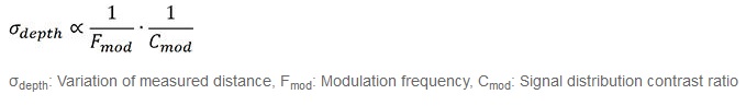
SoftKinetic's CAPD method reads signals at differing phases utilizing light source flight time, multiple times, and then outputs the signal ratio to convert to the distance. Generally, in order to increase the depth map's signal-to-noise ratio (SNR), it is necessary to place multiple readout circuits inside the pixel to read multiple signals at different phases accurately so that the delay of reflected light can be calculated precisely, as well as to improve the usage efficiency of the reflected light signal. Depth measurement accuracy also depends on the capacity to use a faster modulation frequency.
To satisfy all of these requirements, CAPD dynamically creates a potential gradient (slope for electron transfer) and performs high-speed transfer via internal pixel drift current. This design ensures efficient, high-speed transfer of electrons converted from reflected light in the photo detector between two collectors, making it possible to obtain signals of different phases more accurately.
* The depth accuracy is governed by the relationship shown in the following equation.
Highly accurate back-illuminated ToF image sensor with a 10µm pixel pitch, the industry's smallest
ToF pixels generally contain multiple readout circuits inside the pixel, so the multiple transistors and circuitry on top of the photo detector (photodiode) in a front-illuminated CMOS image sensor interfere with reflected light from the object, which brings down distance measurement accuracy.
Sony applied back-illuminated CMOS image sensor pixel technology to improve the effective pixel aperture ratio. This design made the light collection efficiency equivalent to that of a 15µm pixel pitch front-illuminated sensor, but using a back-illuminated sensor with a 10µm pixel pitch. The result is a more compact sensor with more accurate depth-sensing performance. The higher light collection efficiency also made it possible to use a less-power light source, and this kept power consumption down and allowed the sensor module to be even more compact.
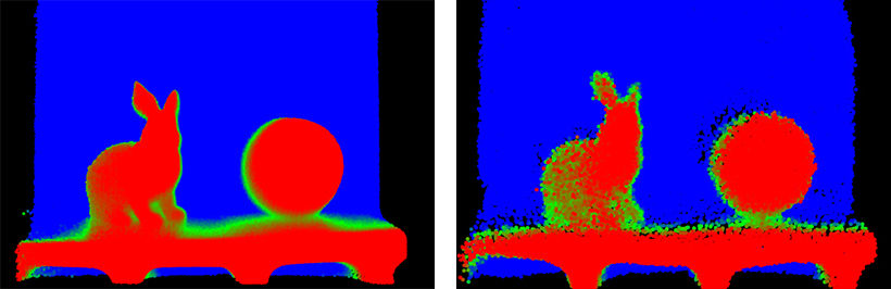
Comparison of obtained depth map at the same distance: New sensor (left) and conventional sensor (right)
In addition, accompanying the adoption of the back-illuminated configuration, the pixel construction and in-pixel circuitry layout were optimized for a ToF sensor, making it possible to accelerate the detection of phase difference required for distance measurement. This made it possible to double the modulation frequency (100 MHz) compared to the conventional method while maintaining the usage efficiency of reflected light, thereby obtaining a better depth map with improved accuracy when measured at the same distance. This in turn provides a depth map just as accurate as conventional methods up to 1.5x further away.
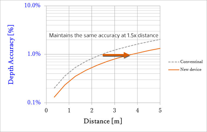
Comparison of measurement distance when the depth accuracy is equivalent (Ambient light: 2k lux; light source power: 104 mW [even]; modulation frequency: 100 MHz)