2017.05.26
A research group consisting of NIMS and university researchers developed versatile spectroscopic microscopy techniques capable of simultaneously measuring a nano-thin film at a wide range of electron energy levels, from almost zero energy to high energy, using a microscope employing electron beams. The group also demonstrated the effectiveness of the technique.
NIMS researchers Bo Da (researcher at the RCAMC and the CMI2, MaDIS) and Hideki Yoshikawa (leader of the Surface Chemical Analysis Group) and a research group led by Shigeo Tanuma (NIMS Special Researcher), Kazuhito Tsukakoshi (MANA Principal Investigator, NIMS), Kazuyuki Watanabe (Professor, Tokyo University of Science) and Zejun Ding (Professor, University of Science and Technology of China) jointly developed versatile spectroscopic microscopy techniques capable of simultaneously measuring a nano-thin film at a wide range of electron energy levels, from almost zero energy to high energy, using a microscope employing electron beams. The group also demonstrated the effectiveness of the technique.
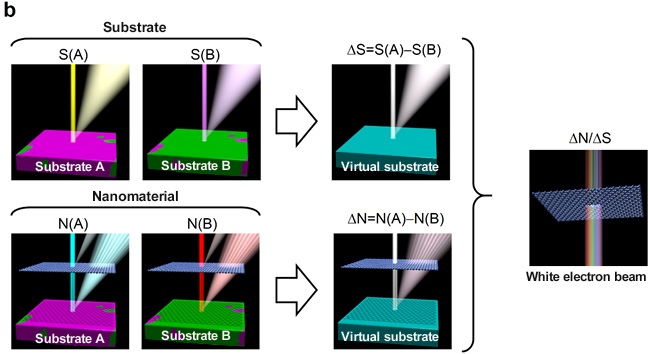
Conventional methods of measuring nano-thin films require great care because they require changing the energy level of a monochromatic incident electron beam and readjusting the electron optical system while measuring the electron microscope image. We addressed this issue using a creative approach. We developed a new measurement technique using secondary electrons—which are generated in a substrate material and have a wide energy distribution—as a virtual white electron probe. To reduce this technique to practice, we needed to completely eliminate background signals from secondary electrons. We adopted the four-point probe method used in astronomy to accurately detect weak signals captured by telescopes. This method enabled us to simultaneously measure the electron transmittance of graphene at a wide range of energy levels between almost zero and 600 electron volts. We then confirmed that the measured values matched well with theoretical values. This study reports for the first time that information on the properties of a material —specifically, the electron transmittance of nano-thin films—can be extracted from secondary electron signals.
Measurement of the transmittance characteristics of a material using visible light of various energy levels is analogous to identifying the color of the material. Similarly, measurement of the electron transmittance of a nano-thin film using electrons of various energy levels is analogous to identifying the color of a localized area of the film using a more narrowly focused “eye” (electrons). It is difficult to quickly determine the quality (e.g., color) of nano-thin films at specific target sites, as the film itself is normally difficult to locate. Accordingly, techniques such as the one developed in this study will be very valuable in research on new nano-thin films in which the qualitative consistency of the film across a large area needs to be ensured.
This research was conducted as a part of the "Materials Research by Information Integration" Initiative (MI2I) supported by the JST’s Support Program for Starting up Innovation Hub, and was conducted using the computer facilities at the Institute for Solid State Physics of the University of Tokyo and the National Institutes of Natural Sciences Okazaki Research Facilities. In addition, this research was funded by MEXT Grants-in-Aid for Scientific Research in the innovative “Science of Atomic Layers” area (No. JP25107004), another Grant-in-Aid for Scientific Research (No. JP25400409) and the National Natural Science Foundation of China (Nos. 11274288 and 11574289).
This study was published in the online version of Nature Communications at 10:00 am on May 26, 2017, local time (6:00 pm on May 26, Japan Time).
(“Virtual substrate method for nanomaterials characterization”; Bo Da, Jiangwei Liu, Mahito Yamamoto, Yoshihiro Ueda, Kazuyuki Watanabe, Nguyen Thanh Cuong, Songlin Li, Kazuhito Tsukagoshi, Hideki Yoshikawa, Hideo Iwai, Shigeo Tanuma, Hongxuan Guo, Zhaoshun Gao, Xia Sun & Zejun Ding; Nature Communications 8, Article number: 15629 (2017); doi:10.1038/ncomms15629)