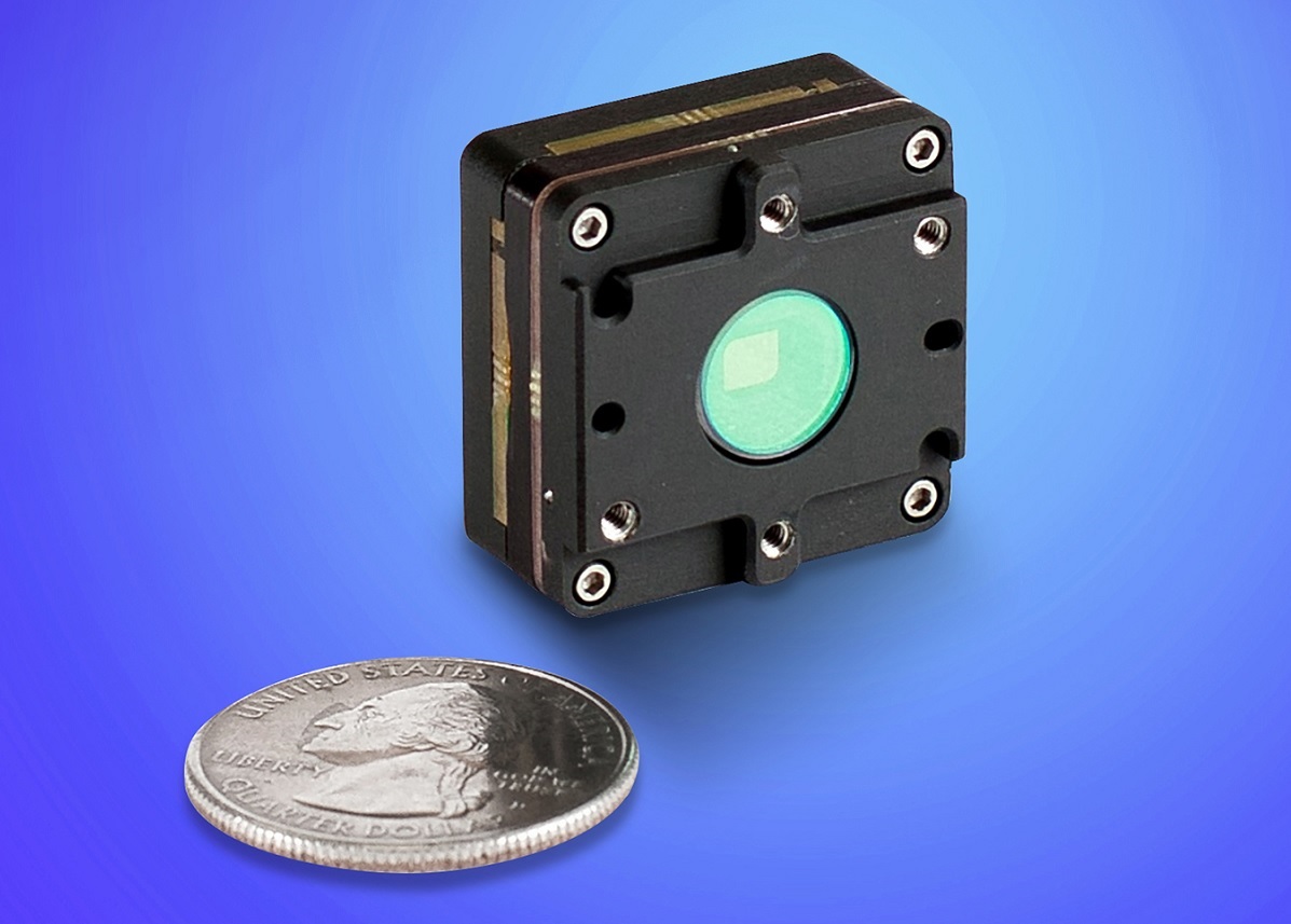
Leuven, Belgium (November 25, 2013) – Imec, the Belgian nanoelectronics research center, will present at this week’s ‘CMOS Image Sensors for High Performance Applications’ workshop in Toulouse (France) a prototype of a high-performance, time-delay-integration (TDI) image sensor. The image sensor is based on imec’s proprietary embedded charge-coupled device (CCD) in CMOS technology. Imec developed and fabricated the sensor for the French Space Agency, CNES, which plans to utilize the technology for space-based earth observation.
The prototype image sensor combines a light-sensitive, CCD-based TDI pixel array with peripheral CMOS readout electronics. By integrating CCD with CMOS technology, imec combined the best of both worlds. The CCD pixel structure delivers low-noise TDI performance in the charge domain, while CMOS technology enables low-power, on-chip integration of fast and complex circuitry readouts.
A TDI imager is a linear device that utilizes a clever synchronization of the linear motion of the scene with multiple samplings of the same image, thereby increasing the signal to noise ratio. CCDs fit extremely well with the TDI application since they operate in the charge domain, enabling the movement of charges without creating excess noise. By combining the TDI pixels array with CMOS readout circuitry on the same die, imec produced a camera-on-a-chip or system-on-a-chip (SOC) imager, which reduces the overall system complexity and cost. The CMOS technology enables on-chip readout electronics, such as clock drivers and analog-to-digital convertors (ADCs), operating at higher speeds and lower power consumption not possible with traditional CCD technology.
The prototypes were fabricated using imec’s 130nm process with an additional CCD process module. An excellent charge transfer efficiency of 99.9987 % has been measured ensuring almost lossless transport of charges in the TDI array, and guaranteeing high image quality. Imec’s specialty imaging platform combines custom design (i.e., specialized pixels, high-performance readout circuits and chip architectures) with optimized silicon processing, such as dedicated implants and backside thinning, to achieve high-end specialized imagers.
About imec
Imec performs world-leading research in nanoelectronics. Imec leverages its scientific knowledge with the innovative power of its global partnerships in ICT, healthcare and energy. Imec delivers industry-relevant technology solutions. In a unique high-tech environment, its international top talent is committed to providing the building blocks for a better life in a sustainable society. Imec is headquartered in Leuven, Belgium, and has offices in Belgium, the Netherlands, Taiwan, US, China, India and Japan. Its staff of close to 2,000 people includes more than 600 industrial residents and guest researchers. In 2011, imec's revenue (P&L) was about 300 million euro. Further information on imec can be found at www.imec.be.