2017.05.24
A research team led by Prof. Mun Seok JEONG of the Dept. of Energy Science at SKKU and Dr. Kyong Duck PARK from University of Colorado in USA successfully revealed twisted bilayer structures of grain boundaries in large-area graphene and identified misorientation angles from correlated analysis of the high resolution multispectral TERS (Tip Enhanced nano Raman Scattering).
Large-area graphene sheets grown by chemical vapor deposition (CVD) have been proposed as a route to realize mass production and commercialization of near-ballistic transport electronic devices. So far, most large-area synthetic graphene is polycrystalline. The associated grain boundaries (GBs) have been identified as a major limitation in device applications due to their modified electronic structure and inhibiting carrier transport. Therefore, understanding the detailed characteristics of GBs is a prerequisite for better design of graphene sheets.
Despite the greater applicability of large-area graphene sheets compared to graphene flakes, most theoretical and experimental studies of GBs have focused on the analysis of atomic defects observed in adjacent crystal faces, which show significant differences from larger scale deformations of GBs in large-area graphene. Scanning tunneling microscopy (STM) and transmission electron microscopy (TEM) can investigate structural defects, electrical conductivity, and strain associated with GBs with atomic scale spatial resolution.
However, these high-resolution local probes provide only a limited field of view, without optical and chemical information. In contrast, Raman spectroscopy and imaging studies of GBs in large-area graphene have shown both an increase and decrease in the G′peak intensity at GBs, and thus have left a confusing picture regarding their lattice structure and vibrational properties, in part due to the diffraction-limited spatial resolution and a low sensitivity of conventional Raman spectroscopy.
In order to complement STM, TEM, and conventional Raman spectroscopy and to bridge their length scales, here they present ≈18 nm spatial resolution tip-enhanced Raman spectroscopy (TERS) and imaging to understand lattice and electronic structure, as well as elastic and phonon scattering properties of GBs in CVD grown large-area graphene. Through correlated analysis of topography, near-field scattering, and multispectral TERS imaging, we reveal bilayer GBs in the form of twisted stacking at the boundary between two misoriented crystal facet. The team also determine the misorientation angles of the bilayer GBs from a detailed quantitative investigation of the Raman G and G′ peak properties, which varying with respect to the misorientation angle associated with the modified electronic structure at the K-point of the Brillouin zone.
Further, they investigate the distinct Raman characteristics from a wrinkle, a different type of line defect. In contrast to the GBs, only the G′ peak exhibits significant changes in intensity with no associated spectral shift in the vicinity of the wrinkle, which directly correlated with a nanoscopic structural curvature effect. From multispectral TERS mapping, they also resolve the chemical variation associated with nucleation sites (NSs), where they confirm AB stacking bilayer structures at the NS and find an unexpected phonon scattering response of the D′ peak, which is associated with sp3-type carbon hybridization defects.
Beyond the newly revealed properties of the defects, these results may provide clues to understand the growth mechanism of large-area graphene and the formation of nanoscale defects. Furthermore, their work demonstrates the potential of correlated analysis of multispectral TERS imaging as a generally applicable approach for the investigation of the wide range of 2D materials beyond graphene.
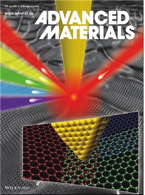
The results of this study were published in the world's leading authoritative journal formaterials engineering field Advanced Materials as of February 17th, 2017 and selected as an inside back cover article.


