Feb. 07, 2017
FAYETTEVILLE, Ark. – A multi-institutional team of researchers, led by University of Arkansas engineering professor Shui-Qing “Fisher” Yu and a leading semiconductor equipment manufacturer, have fabricated an “optically pumped” laser made of the alloy germanium tin grown on silicon substrates.
The augmented material could lead to the development of fully integrated silicon photonics, including both circuits and lasers, and thus faster micro-processing speed at much lower cost.
The researchers’ findings were published in Applied Physics Letters.
Germanium tin holds great promise as a semiconducting material for future optical integration of computer chips, because it harnesses efficient emission of light, which silicon, the standard material for making computer chips, cannot do. In recent years, materials scientists and engineers, including Yu and several of his colleagues on this project, have focused on the development of germanium tin, grown on silicon substrates, to build a so-called optoelectronics “superchip” that can transmit data much faster than current chips.
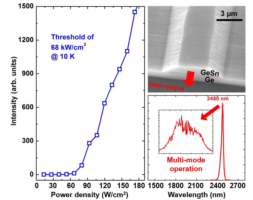
Yu and his colleagues’ most recent contribution to this effort is an optically pumped laser using germanium tin. Optically pumped means the material is injected with light, similar to an injection of electrical current.
“We reduced the laser threshold 80 percent at a lasing operation temperature up to 110 Kelvin,” Yu said. “This is significant progress compared with the previously reported best result and shows that germanium tin holds great promise as an on-chip laser.”
The temperature 110 Kelvin is equal to about –261 Fahrenheit.
On this project, Yu and his colleagues worked with ASM America Inc.’s research and development staff, who developed the growth methods. ASM’s methods produce low-cost and high-quality germanium tin in an industry standard chemical vapor deposition reactor.
In addition to Yu, the research team includes John Tolle, epitaxy research and development manager at ASM; Joe Margetis, epitaxy engineer at ASM; Hameed Naseem, professor of electrical engineering at the University of Arkansas; Mansour Mortazavi, professor of chemistry at the University of Arkansas at Pine Bluff; Wei Du, professor of physics at the University of Arkansas at Pine Bluff; Baohua Li, CEO of Arktonics LLC; Jifeng Liu, professor of engineering at Dartmouth College; and Richard Soref (recognized as “the father of silicon photonics”) and Greg Sun, professors of engineering at the University of Massachusetts Boston.
The University of Arkansas’ researchers are supported by the Air Force Office of Scientific Research and the National Science Foundation.
Paper:
An optically pumped 2.5 μm GeSn laser on Si operating at 110 K
http://aip.scitation.org/doi/abs/10.1063/1.4966141?journalCode=apl