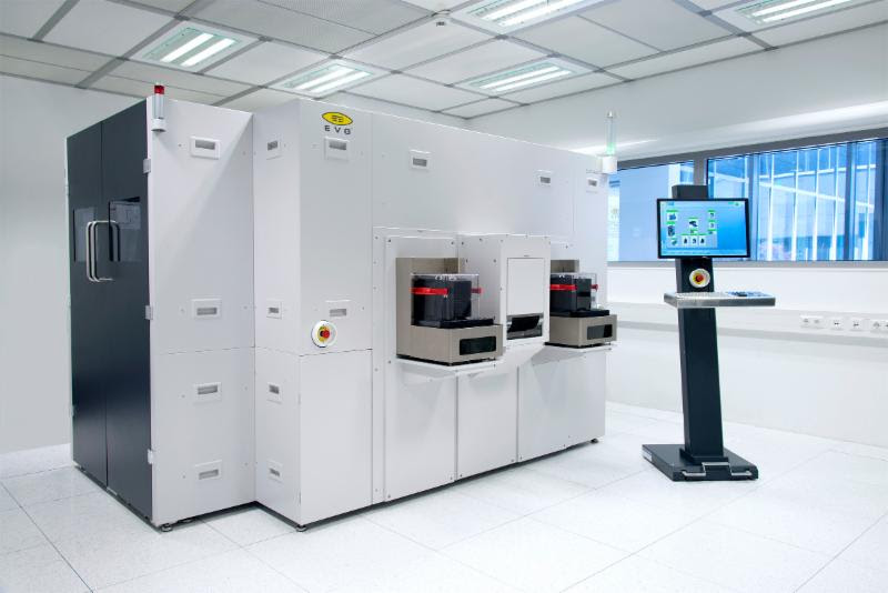
ST. FLORIAN, Austria, July 5, 2017--EV Group (EVG), a leading supplier of wafer bonding and lithography equipment for the MEMS, nanotechnology and semiconductor markets, today unveiled its next-generation laser debonding solution, which enables high-throughput, low-cost-of-ownership (CoO) room-temperature debonding for ultra-thin and stacked fan-out packages. Designed as a module for integration in the company's benchmark EVG®850 DB automated debonding system, the new laser debonding solution incorporates a solid-state laser and proprietary beam-shaping optics to enable optimized, force-free debonding. Featuring both low-temperature debonding and high-temperature-processing stability, EVG's new laser debonding solution is ideal not only for fan-out wafer-level packaging (FoWLP), but also for processing compound semiconductors and power devices. System orders have already been placed for the new solution.
"The semiconductor industry and its touch points grow more diverse by the day. The Internet of Things, automotive advancements, communications and virtual needs are now all being driven by the advancements in this industry," stated Paul Lindner, executive technology director at EV Group. "Many of these developments are now taking place at the packaging level, where the need for greater device functionality and smaller form factors has led to more complex packages, stacked packages, systems in package, as well as high-performance packages. EVG's temporary bonding and debonding solutions, including our latest-generation laser debonding module, play a crucial role in enabling wafer thinning to address the smaller form factors required for these new packaging architectures and applications."
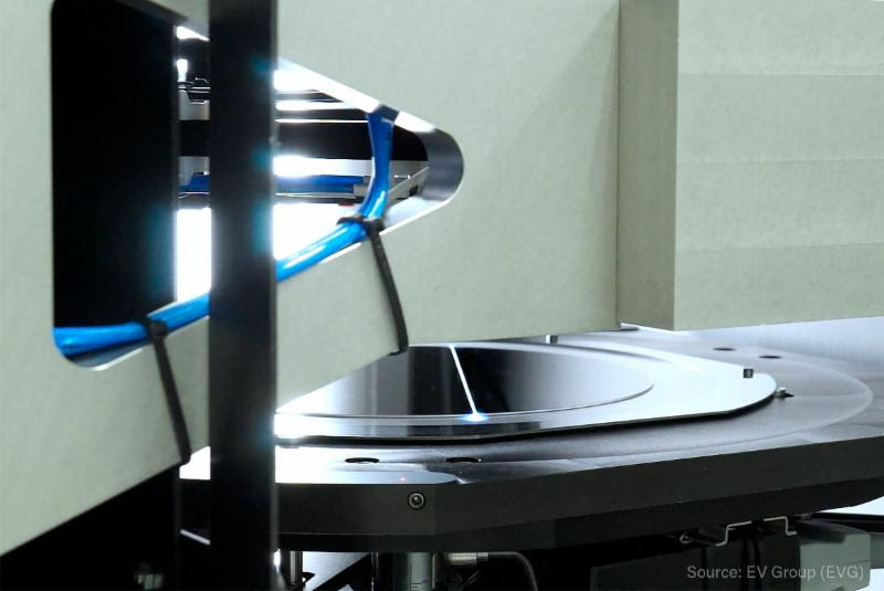
Close up of EVG's next-generation laser debonding module with solid-state UV laser scanning across the surface of a fixed wafer.
FoWLP offers the ability to enable very thin devices and system integration with increased performance, functionality and design flexibility for consumer and mobile handheld devices. According to market research and strategy consulting firm Yole Développement, FoWLP is growing at a compound annual growth rate (CAGR) of 36 percent from 2017 to 2022, reaching more than $3 billion in 2022.* The extreme thinness of device wafers in FoWLP is driving the need for temporary carrier technologies. In the case of the "chip last / redistribution layer (RDL) first" FoWLP approach, the entire package flow occurs on a glass wafer or glass panel. Since the RDL layer is immediately on top of the debonding layer, low force is essential to minimizing risk of yield loss during the debonding process. Laser debonding is ideally suited to remove the glass handler after RDL formation due to its use of minimum force. In addition, the temperature stability of the laser debonding process allows it to easily remove bonding adhesive materials without impacting other materials in the package. The result is high process yield and low risk of device wafer breakage.
Top to Bottom Enhancements for Improved Laser Debonding Yield and CoO
EVG's new laser debonding solution incorporates a solid-state UV laser and a proprietary optical setup that shapes the Gaussian beam profile of the laser into a "quasi top hat" beam profile. By employing this optical setup, EVG achieves a highly reproducible beam with minimal heat introduced to the device wafer and excellent spatial control. This enables tighter process control, which coupled with the high pulse repetition rate of the laser, the ability to conduct laser treatment and wafer separation in a single chamber to minimize handling time, and the ability to scan across the surface of a fixed wafer, leads to a well-controlled, high-throughput and low-temperature debonding process.
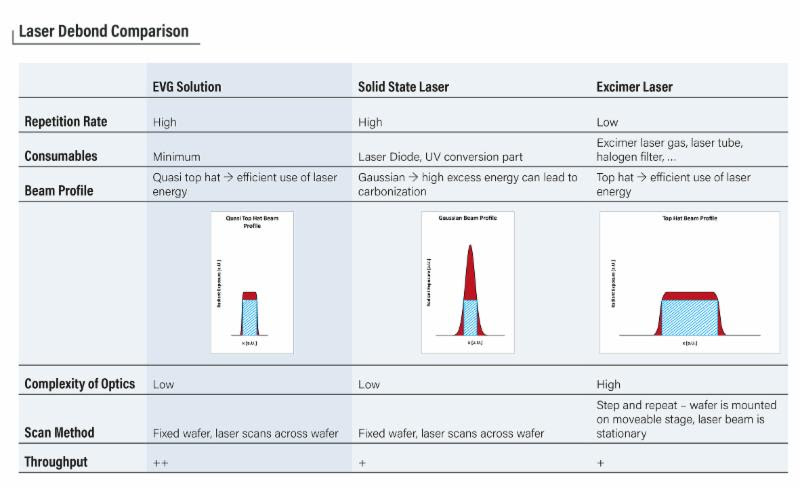
Comparison of three laser types (from left to right) advanced: UV laser solution from EVG; (2) conventional solid-state laser; and (3) excimer laser. The blue crisscross areas in the beam profile image indicate the radiant exposure used for the laser debond process while the red area indicates energy that cannot be used for debonding. The EVG laser debonding solution combines the best features of both other laser types.
Low laser maintenance, high carrier wafer lifetime, the ability to support fully automated handling on film frame, oversized carriers or free standing / unsupported thin wafers, and optimized footprint layout, all round out the system's low CoO advantages. In the tradition of EVG's open platform approach to wafer bonding, the laser debonding solution is also compatible with a wide variety of commercially available adhesive materials.
Product demonstrations of the new laser debonding solution are now available at EVG's cleanroom facilities.
EVG will showcase its new laser debonding solution, along with its complete suite of wafer bonding, lithography and resist processing solutions for advanced packaging applications, at SEMICON West, to be held July 11-13 at the Moscone Convention Center in San Francisco, Calif. Attendees interested in learning more can visit EVG at Booth #7211 in the West Hall.
More information on the new laser debonding solution is also available at: www.evgroup.com/en/products/bonding/temporary_bonding/evg850autodebond/
* Note to Editors: The source for this market data is the "Status of the Advanced Packaging Industry 2017" report, released by Yole Développement in May 2017. More information on the report is available at: https://www.i-micronews.com/advanced-packaging-report/product/status-of-the-advanced-packaging-industry-2017
About EV Group (EVG)
EV Group (EVG) is a leading supplier of equipment and process solutions for the manufacture of semiconductors, microelectromechanical systems (MEMS), compound semiconductors, power devices and nanotechnology devices. Key products include wafer bonding, thin-wafer processing, lithography/nanoimprint lithography (NIL) and metrology equipment, as well as photoresist coaters, cleaners and inspection systems. Founded in 1980, EV Group services and supports an elaborate network of global customers and partners all over the world. More information about EVG is available at www.EVGroup.com.