2016-12-06
Researchers at the Gwangju Institute of Science and Technology (GIST) have developed a semiconductor mesh that will allow for the creation of highly transparent electronic devices to bend freely as seen in movies.
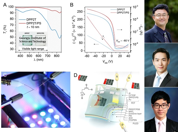
The National Research Foundation of Korea (NRF) has announced that Professor Kwanghee Lee's research team at the Gwangju Institute of Science and Technology (GIST) has successfully developed a new net-structure organic semiconductor material (semiconducting materials using organic materials, such as monomers and polymers containing carbon) that can be made into a thin film (Thin film with nanometer scale) through an easy solution process, and is able to bend freely with a visible light transmittance close to 100%.
Currently, semiconductor materials are excellent in flexibility but do not have perfect visible light transmittance. Organic polymer semiconductors, which have been spotlighted as flexible semiconductor materials, have limitations in making them transparent because of their unique absorption properties of visible light.
The GIST research team then introduced a small amount of polymer semiconductors into a transparent insulator polymer in the visible light region to realize a polymer semiconductor having a structure like a net.
This semiconductor/insulator polymer combination has improved the charge mobility by about 4 times compared to that of a pure thin film type in which a polymer semiconductor. The visible light transmittance is close to 100% due to its structural characteristic, such as a very thin mesh, through which objects on the opposite side can be seen without color distortion through the semiconductor thin film.
Professor Kwanghee Lee said, "The results of this research exceeded the possibilities of organic materials as electronic materials and implemented the functions that many have dreamed of. This new paradigm of semiconductor technology, along with the transparency of ultra-thin films, which cannot be realized with existing silicon technology, has provide a way to realize new electronic devices, such as aesthetically superior wearable devices."
The results of this research have been carried out with the support of the Ministry of Science, ICT and Future Planning Basic Research Program (individual research), and it was published in the Proceedings of the National Academy of Sciences (PNAS) on November 22, 2016.


