25.04.2016
By optimizing the temporal structure of ultrashort laser pulses German scientists achieved high-aspect ratio nano-machining of fused silica. At the optical wavelength of 800 nanometers holes only 250 na-nometers wide but up to seven micrometers deep were demonstrated.
Nanotechnology is at the forefront of today’s advance in areas such as electronics, optical communica-tion and biomedicine. It is about custom-designed structures that are smaller than a micrometer which is already a hundredth of the diameter of a human hair. These so-called nanostructures exhibit proper-ties unknown from larger specimen of the same material. Fabrication of such systems is still a challenge with many different techniques available.
A direct approach to write the desired structures on a substrate is to remove unwanted material by evap-oration in an intense laser field. However, there are severe limitations. First of all, intense lasers interact mostly with the surface of most materials. Additionally, the minimum spot size and, consequently, the smallest structure written by a laser beam is given by the wavelength of the radiation. For visible light this is 400 to 800 nanometers which today is above the size of some electronic components.
Physicists and electrical engineers of the Center for Interdisciplinary Nanostructure Science and Tech-nology (CINSaT) at the University of Kassel in Germany now demonstrated the creation of sub-focal nano-holes in fused silica with a diameter below 250 nanometers at a wavelength of 800 nanometers. At the same times these holes reach up to seven micrometers deep into the glass providing an aspect ratio that is otherwise difficult to achieve on such small structures.
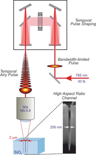
The team led by Thomas Baumert and Hartmut Hillmer uses laser pulses that are only around one part in a trillion seconds short. But this alone does not do the trick. Using a home-built pulse shaping tech-nique they create optimized sequences of light – so-called temporal Airy pulses (see image 1) – that are structured such that they efficiently excite the material. This efficient excitation is not instantaneous but a delayed, avalanche-like process. Consequently, the laser pulses are not the shor-test possible ones but stretched to optimal length. The delayed ionization mechanism also circumvents the above-mentioned problem that most of the pulse is absorbed at the surface of the material. Instead excitation is carried into the material, leading to deep and narrow channels. Carefully adjusting the pulse sequence enables to change the depth of the created holes, but also the size of the focal spot and its position with respect to the surface are important control parameters. Interestingly, the approach does not use ex-tremely high laser powers, where non-linear effects such as self-focusing could explain the observed spatial narrowing of the material modification.
The scientists in Kassel are currently testing the technique for the production of miniaturized filters in optical communications. Other possible applications are nano-surgery and cell poration.
Link to the original publication:
http://www.osapublishing.org/optica/abstract.cfm?uri=optica-3-4-389